Multi-threshold MIS integrated circuit device and circuit design method thereof

a technology of integrated circuit device and multi-threshold voltage, which is applied in the direction of logic circuit coupling/interface arrangement, instruments, transistors, etc., can solve the problems of reducing the operating speed of mos transistors, difficult to achieve the reduction of power consumption, and excessive margin in the entire circuit, so as to reduce the design time of multi-threshold mis integrated circuit devices

Inactive Publication Date: 2005-05-31
SOCIONEXT INC
View PDF13 Cites 42 Cited by
  • Summary
  • Abstract
  • Description
  • Claims
  • Application Information

AI Technical Summary

Benefits of technology

[0016]According to this configuration, a power supply line of the macro that does not include a virtual power supply line and a leak-current-shielding MIS transistor can be used as a virtual power supply line. In addition this allows reducing the design time of a multi-threshold MIS integrated circuit device. Further, the size such as length of the leak-current-shielding MIS transistor cell is suitably determined according to the current consumption of the macro, so as to repress increase of the macro-occupied area on the substrate as compared with the prior art.

Problems solved by technology

However, lowering the power source voltage leads to lowering the operating speed of MOS transistors.
However, lowering the threshold voltage causes increase in leakage current of MOS transistor in standby time, consequently making it difficult to achieve the lower power consumption.
In addition, in the case of the circuit shown in FIG. 9, because the gate width of the leak-current-shielding MOS transistor is determined by considering a margin in current flowing through the logic gate, in order not to hinder the improvement of speed for each logic gate, the margin in the entire circuit becomes excessively large, increasing the macro-occupied area on the substrate.
In case of the circuit shown in FIG. 10, because no logic gate is included in the leak-current-shielding cell, useless area becomes increased, thereby increasing the macro-occupied area on the substrate.

Method used


Image

  • Multi-threshold MIS integrated circuit device and circuit design method thereof
  • Multi-threshold MIS integrated circuit device and circuit design method thereof
  • Multi-threshold MIS integrated circuit device and circuit design method thereof

Examples


first embodiment

[0028

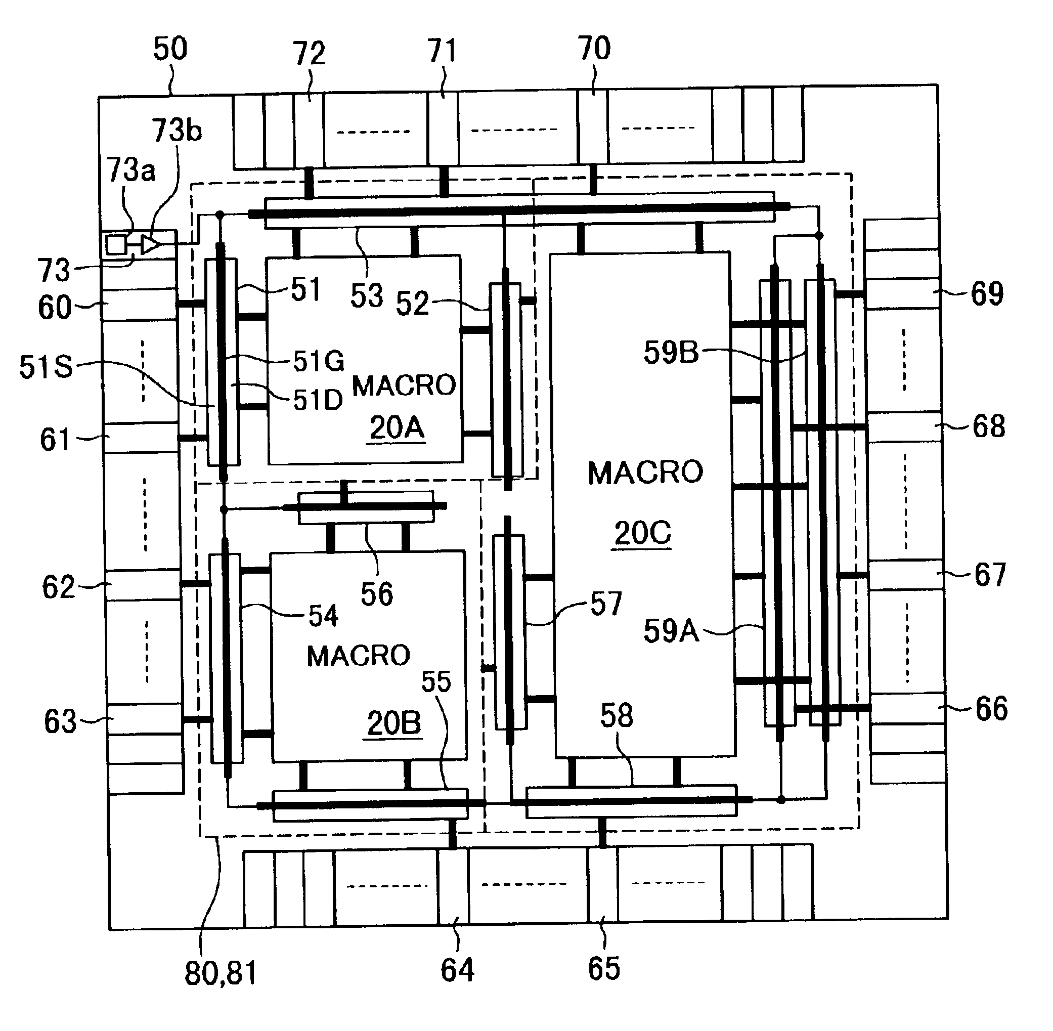
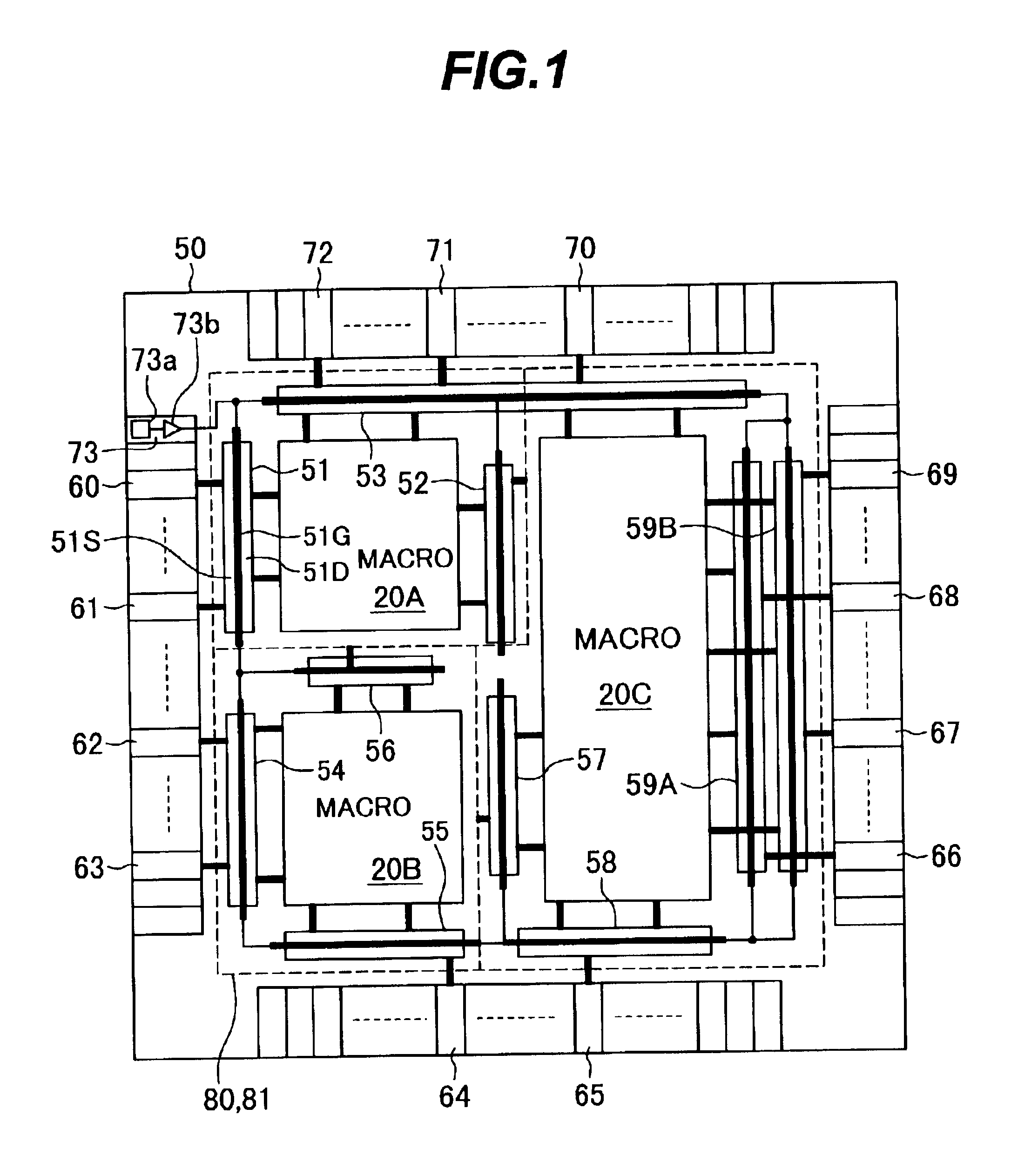
[0029]FIG. 1 is a schematic on-chip layout view of a multi-threshold voltage MOS integrated circuit device according to a first embodiment of the present invention.

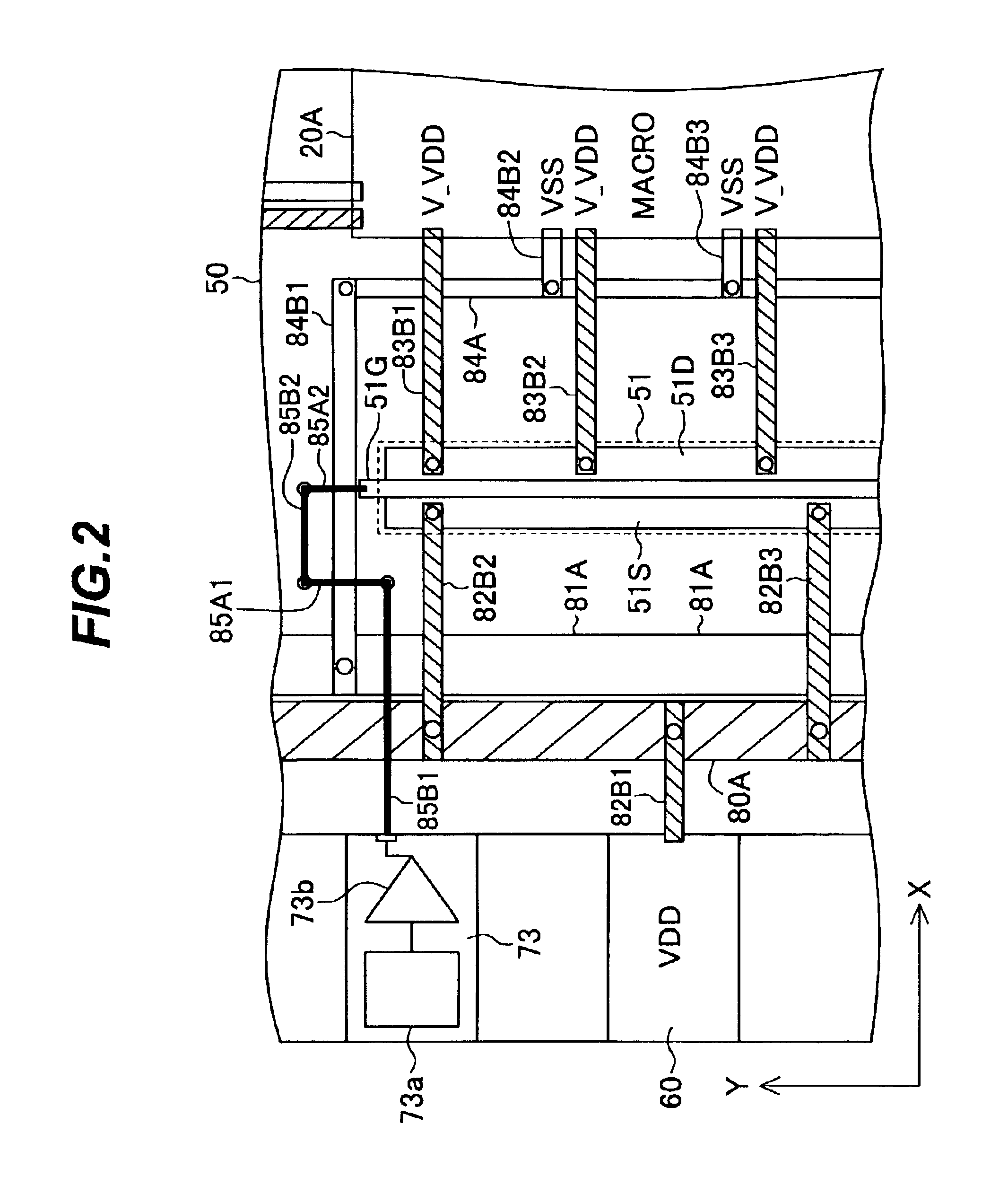
[0030]Macros 20A, 20B and 20C are disposed on a semiconductor chip 50, and any of them do not have the leak-current-shielding circuit shown in FIG. 7(A) or 7(B), but are, for example, ones purchased as IP from other companies. Macros 20A, 20B and 20C are, for example, a memory, a DSP (Digital Signal Processor), and a CPU, respectively. According to the present invention, determination on whether or not using supply lines of power source voltages VDD and VSS in the macro 20A to 20C as supply lines of virtual power source voltages V_VDD and V_VSS, respectively, is determined according to whether or not connecting these lines with leak-current-shielding circuits independent from these lines. In the first embodiment, because the VDD supply lines in the macros 20A to 20C are used as V_VDD supply lines, VDD is denoted by V...

second embodiment

[0043

[0044]FIG. 4 is a schematic on-chip layout view of a multi-threshold voltage MOS integrated circuit device, according to a second embodiment of the present invention.

[0045]In this semiconductor chip 50A, the power source voltages VDD and VSS are directly supplied to a macro 20D from VDD pads for external connection. The macro 20D is not provided with a power source shielding MOS transistor of a high threshold voltage. The macro 20D outputs a power control signal *PCNT through a terminal that is connected through a control signal line 90 to gate lines of a PMOS transistor cells 51 to 53 and 57 to 59B. Using the power control signal *PCNT, the macro 20D performs on / off controls of the PMOS transistor cells 51 to 53 and 57 to 59B, according to external signal or internal state.

[0046]The others are the same as the first embodiment.

third embodiment

[0047

[0048]FIG. 5 is a schematic on-chip layout view of a multi-threshold voltage MOS integrated circuit device according to a third embodiment of the present invention.

[0049]In this semiconductor chip 50B, in stead of the leak-current-shielding PMOS transistor cell 51 of FIG. 4, disposed along a side of the macro-frame of the macro 20A, there are arranged PMOS transistor cells 511 to 513 in predetermined length, for example 100 μm, which are registered in a cell library. Gate lines of neighboring PMOS transistors 511 to 513 are connected to each other. The necessary number of PMOS transistor cells 511 to 513 for the macro 20A is determined based on the current consumption of the macro 20A in active time. The same applies to the other PMOS transistor cells. Exception is that those corresponding to the PMOS transistor cell 59B of FIG. 4 are omitted in FIG. 5.

[0050]The others are the same as the second embodiment.

[0051]The third embodiment allows forming the leak-current-shielding PMO...


PUM


Abstract

On a chip 50A, disposed are macro cell 20A not including a virtual power supply line and a leak-current-shielding MOS transistor of a high threshold voltage, and a leak-current-shielding MOS transistor cell 51 of the high threshold voltage. The transistor cell 51 has a gate line 51G which is coincident with the longitudinal direction of the cell, is disposed along a side of a rectangular cell frame of the macro cell 20A, and has a drain region 51D connected to VDD pads 60 and 61 for external connection, the gate line 51G connected to an I/O cell 73 and a source region 51S connected to a VDD terminal of the macro cell 20A. This VDD terminal functions as a terminal of a virtual power supply line V_VDD.

Description

BACKGROUND OF THE INVENTION[0001]1. Field of the Invention[0002]The present invention relates to a MIS integrated circuit device of multi-threshold voltage and a circuit design method thereof, and particularly to a MIS (Metal Insulator Semiconductor), more particularly to a CMOS (Complementary Metal Oxide Semiconductor) integrated circuit device of multi-threshold voltage, which is provided with a circuit including a MIS transistor of a low threshold voltage and a MIS transistor of a high threshold voltage for shielding a leak current flowing through the circuit in standby time, and a circuit design method thereof.[0003]2. Description of the Related Art[0004]Recently, there has been a demand for higher speed potable electronic devices and their lower power consumption for long battery life. In CMOS LSIs, because power consumption is proportional to the square of voltage, reducing the power consumption can be achieved by lowering the power source voltage. However, lowering the power ...

Claims


Application Information

Patent Timeline
Patent Type & Authority Patents(United States)
IPC IPC(8): H01L29/76H01L21/70H01L21/822H01L29/66H01L21/82H01L21/8238H01L27/085H01L27/10H01L27/092H01L27/118H03K19/0175H01L27/04G11C11/00G11C11/40
CPCH01L27/11807G11C11/40
Inventor MIYAGI, SATORU
Owner SOCIONEXT INC
Why Eureka
Try Eureka