Current-voltage conversion circuit

a voltage conversion circuit and current voltage technology, applied in the field of current voltage conversion circuits, can solve the problems of non-uniform and non-uniform duty ratios of high level and low level, distortion of voltage signal that is input into the inverter, etc., and achieve the effect of reducing the distortion of the waveform of the voltage signal that is input into the amplifying inverter and high sensitivity

Inactive Publication Date: 2005-05-31
LAPIS SEMICON CO LTD
View PDF7 Cites 1 Cited by
  • Summary
  • Abstract
  • Description
  • Claims
  • Application Information

AI Technical Summary

Benefits of technology

[0016]In this case, the source-drain resistance varies in inverse proportion to the amplitude of the input signal. Furthermore, the current-voltage characteristics of the transistor disposed inside the feedback inverter vary according to the gate voltage. Accordingly, the current-voltage conversion circuit of the present invention can vary the current-voltage characteristics of the feedback inverter in accordance with the amplitude of the input signal; as a result, an effect equivalent to that obtained when the resistance value of the resistance element 708 in a conventional feedback circuit is made variable can be achieved.
[0017]In the current-voltage conversion circuit of the present inven

Problems solved by technology

As a result, amplification will be performed on an input signal in which the ratios of the high level and low level are non-uniform (non-uniform duty ratio).
However, in cases where the inverters 703 through 705 of the current-voltage conversion circui

Method used


Image

  • Current-voltage conversion circuit
  • Current-voltage conversion circuit
  • Current-voltage conversion circuit

Examples


first embodiment

[0035]A current-voltage conversion circuit constituting the present invention will be described with reference to FIGS. 1 through 3.

[0036]FIG. 1 is a circuit diagram which shows the overall construction of the current-voltage conversion circuit of the present embodiment.

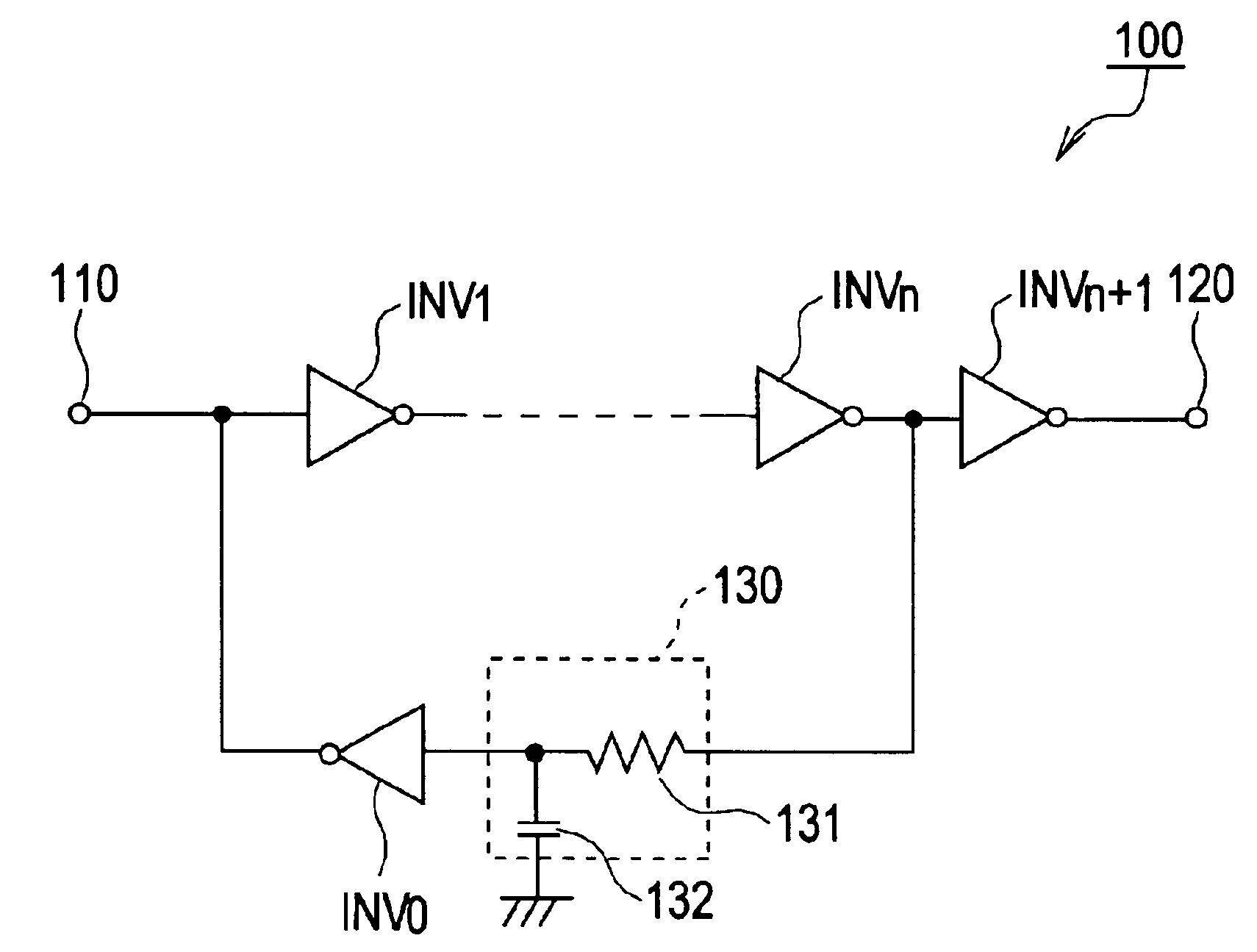
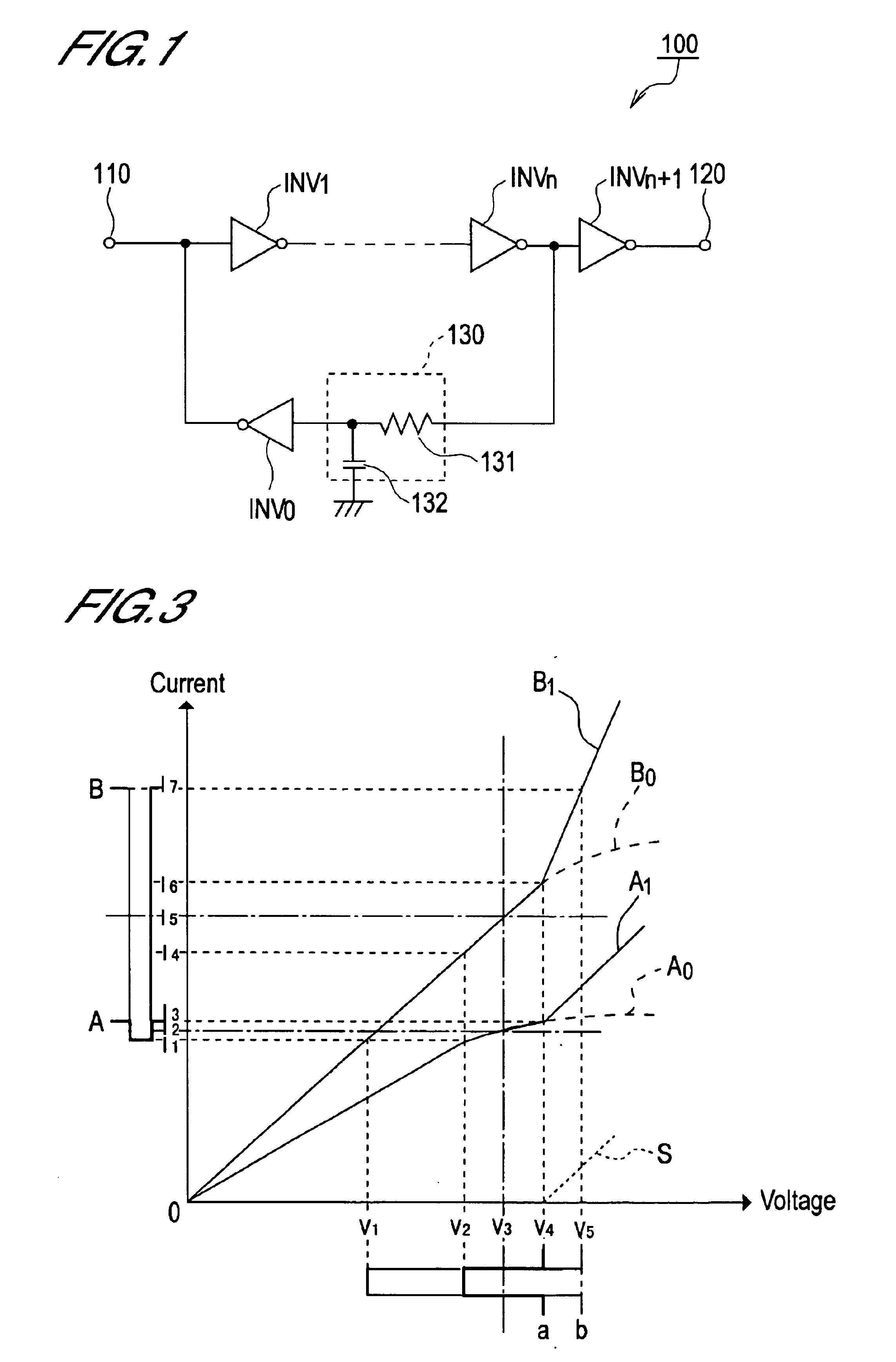
[0037]As is shown in FIG. 1, this current-voltage conversion circuit 100 comprises a signal input terminal 110, amplifying inverters INV1 through INVn+1, an output terminal 120, an integrating circuit 130, and a feedback inverter INV0.

[0038]The input terminal 110 inputs a current signal from the outside.

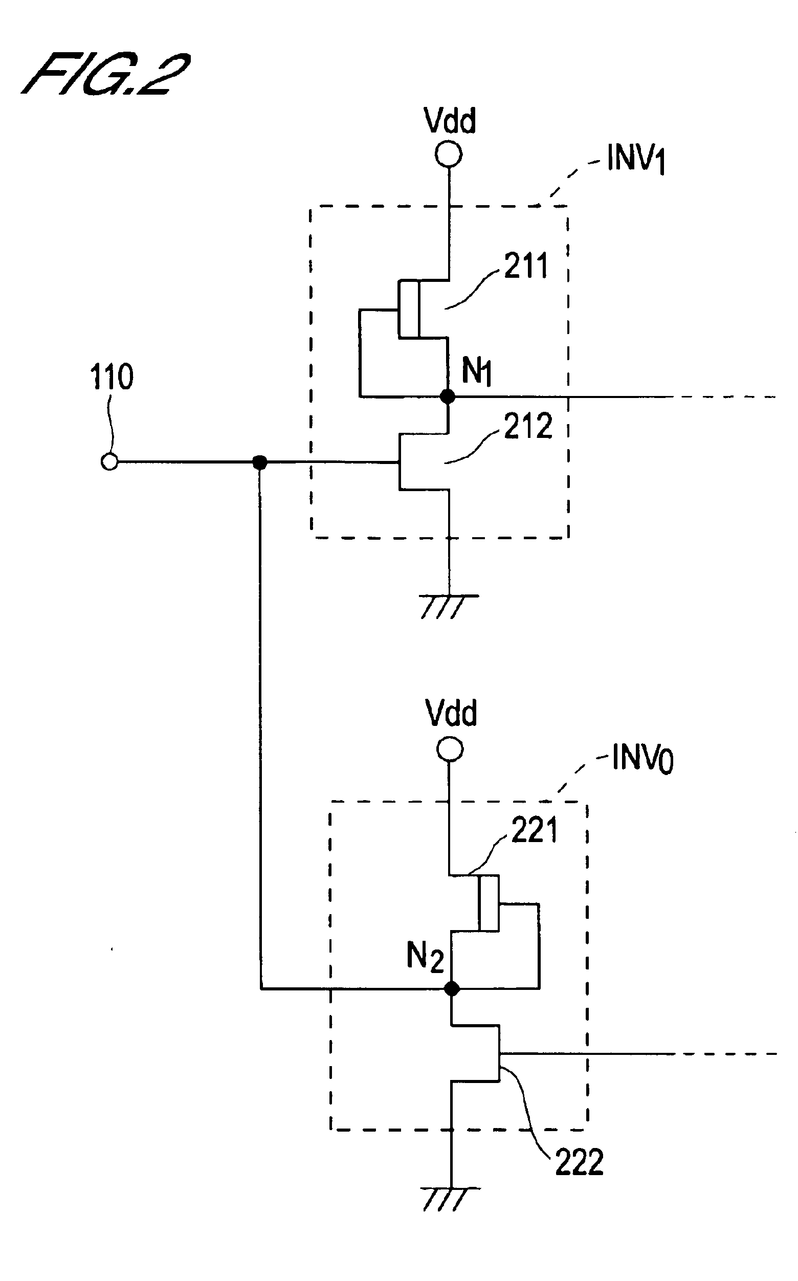
[0039]The amplifying inverters INV1 through INVn+1 are connected in series. The input of the first-stage amplifying inverter INV1 is connected to the input terminal 110. Furthermore, the output of the final-stage amplifying inverter INVn+1 is connected to the output terminal 120. In the present embodiment, n is an even number.

[0040]The integrating circuit 130 comprises a resistance element 131 and a capacitor 132. One...


PUM


Abstract

It is an object of the present invention to provide a current-voltage conversion circuit in which the sensitivity varies in accordance with the amplitude of the input signal. In the current-voltage conversion circuit of the present invention, n+1 (n is an even number) amplifying inverters are connected in series between an input terminal and an output terminal; furthermore, the input of a negative feedback circuit constructed from an integrating circuit and a negative feedback inverter is connected to the output side of the nth-stage amplifying inverter, and the output of this negative feedback circuit is connected to the input side of the first-stage amplifying inverter. The integrating circuit outputs the mean value of the output potential of the nth-stage amplifying inverter into the negative feedback inverter, and the negative feedback inverter controls the current that flows the ground line from the input terminal in accordance with the output voltage of the integrating circuit. As a result, the sensitivity of the current-voltage conversion circuit varies accordingly.

Description

BACKGROUND OF THE INVENTION[0001]1. Field of the Invention[0002]The present invention relates to a current-voltage conversion circuit, and more particularly to a current-voltage conversion circuit with a limiting function which is used for example in optical communications or the like. This application is a counterpart application of Japanese application Serial Number 180763 / 2002, filed Jun. 21, 2002, the subject matter of which is incorporated herein by reference.[0003]2. Description of the Related Art[0004]Current-voltage conversion circuits contain signal amplifiers used in various applications. A limiting amplifier which is used for example in the relays of optical communications systems or the like is known as one type of signal amplifier. Known amplifiers of this type include (for example) the limiting amplifier disclosed by Murayama et al. in “10 Gb / s Low Power Limiting Amplifier for Optical Communication Systems” (Electronics Society Conference of the Electronic Information ...

Claims


Application Information

Patent Timeline
IPC IPC(8): H03G3/30H03F3/08H03F1/34
CPCH03G3/3084
Inventor YAMADA, HIROYUKITAMURA, SHIGEYUKIIKEMURA, KUNIICHI
Owner LAPIS SEMICON CO LTD
Why Eureka
Try Eureka