Clock generator for generating accurate and low-jitter clock

a clock generator and clock technology, applied in the field of clocks, can solve the problems of affecting the performance of the chip, the speed gap is becoming a bottleneck limiting the performance improvement of the computer as a whole, and the speed of signal transmission between elements or circuit blocks within the chip is becoming a major factor limiting the chip performance, etc., to achieve the effect of generating an accurate, low jitter clock

Active Publication Date: 2005-05-31
FUJITSU LTD
View PDF12 Cites 74 Cited by
  • Summary
  • Abstract
  • Description
  • Claims
  • Application Information

AI Technical Summary

Benefits of technology

[0010]An object of the present invention is to provide a clock generator that can generate an accurate, low jitter clock, whether when generating an intern

Problems solved by technology

The improvements in the performance of semiconductor memory devices, processors, and the like have reached the point where system performance cannot be improved further unless the speed of signal transmission between components or elements is increased.
Specifically, the speed gap between a DRAM and a processor (i.e., between LSIs), for example, has been widening year by year and, in recent years, this speed gap has been becoming a bottleneck impeding performance improvement for a computer as a whole.
Furthermore, with increasing int

Method used


Image

  • Clock generator for generating accurate and low-jitter clock
  • Clock generator for generating accurate and low-jitter clock
  • Clock generator for generating accurate and low-jitter clock

Examples


first embodiment

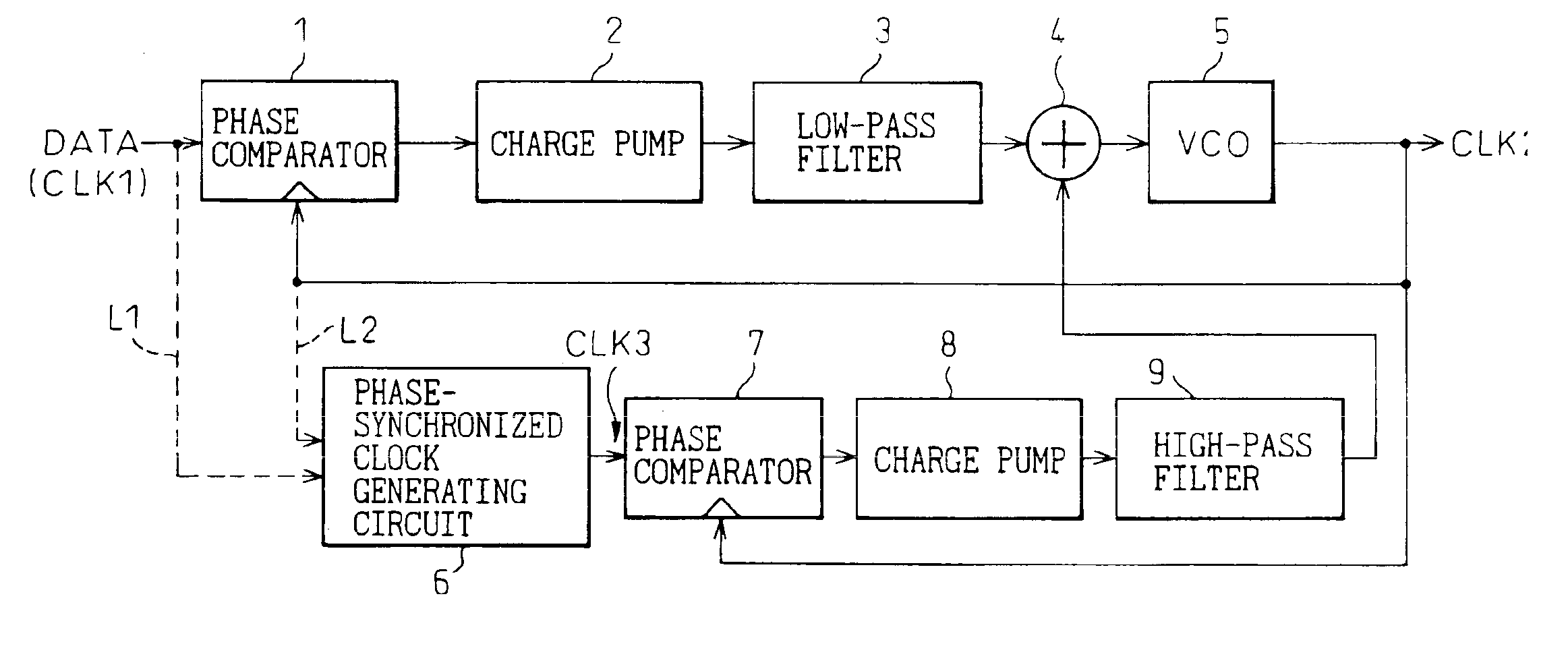
[0048]FIG. 3 is a block diagram showing the clock generator according to the present invention. In FIG. 3, reference numerals 1 and 7 are phase comparators, 2 and 8 are charge pumps, 4 is an adder, 5 is a VCO (Voltage Controlled Oscillator), 6 is a multiply-by-2 circuit (phase-synchronized clock generating circuit), 9 is a high-pass filter, 10 is a processing circuit, and 11 is a control signal generating circuit.

[0049]As shown in FIG. 3, in the clock generator of the first embodiment, the phase comparator 1 compares the phase of the external clock CLK 1 (or the input data DATA) with the phase of the internal clock CLK 2 output from the VCO 5, while the phase comparator 7 compares the phase of the external clock multiplied by 2 by the multiply-by-2 circuit 6 (the phase of the comparison clock CLK 3) with the phase of the internal clock CLK 2.

[0050]The outputs of the phase comparators 1 and 7 are supplied to the control signal generating circuit 11, and the VCO 5 is controlled by the...

second embodiment

[0055]FIG. 5 is a block diagram showing the clock generator according to the present invention, in which an internal clock synchronized to externally supplied data is generated. In FIG. 5, reference numeral 21 is a flip-flop circuit (FF circuit), 22 and 23 are phase comparators, 24 is a control voltage generating circuit (control signal generating circuit), and 25 is a VCO.

[0056]In the clock generator of the foregoing first embodiment shown in FIG. 3, the phase-synchronized clock is generated at the receiving side, but in the clock generator of the second embodiment shown in FIG. 5, the phase-synchronized clock is generated at the transmitting side. More specifically, the driving clock for the FF circuit 21 used in the circuit for generating the output data is used as the data clock D-CLK and is transmitted together with the data. At the receiving side, the phase comparator 22 compares the phase of the internal clock CLK 2 (the output clock of the VCO 25) with the phase of the data ...

third embodiment

[0059]FIG. 6 is a block diagram conceptually showing the clock generator according to the present invention. In FIG. 6, reference numerals 31 and 41-0 to 41-n are adders (subtractors); 32 and 42-0 to 42-n are receiver / phase comparators (phase detectors); 33 and 43-0 to 43-n are phase interpolators (PIs); 34, 39, and 44-0 to 44-n are coefficient multipliers; 35, 37, 45-0 to 45-n, and 47-0 to 47-n are adders; 36 is a frequency register (integrator circuit); 38 is a phase register (integrator circuit); 40 is a high-pass filter; and 46-0 to 46-n are registers. Here, the frequency register 36 and the phase register 38 can be constructed using, for example, an adder and an accumulator.

[0060]The coefficient multiplier 34 multiplies the output of the receiver / phase detector 32 by a coefficient g1 and supplies the result to the adder 35, the coefficient multiplier 39 multiplies the output of the receiver / phase detector 32 by a coefficient g2 and supplies the result to the adder 37, and the c...


PUM


Abstract

A clock generator has a clock generating circuit, a phase difference detection circuit, and a control signal generating circuit. The clock generating circuit has a function for varying a clock phase in accordance with a control signal, the phase difference detection circuit compars the clock phase output from the clock generating circuit with a phase of a reference waveform, and detecting a phase difference therebetween, and the control signal generating circuit generates a control signal for controlling the clock phase of the clock generating circuit, based on phase difference information obtained from the phase difference detection circuit. The phase difference detection circuit has a plurality of phase detection units, at least one of the plurality of phase detection units carries out a direct phase detection in which a phase of the clock is directly compared with the phase of the reference waveform, and at least the other one of the plurality of phase detection units carries out an indirect phase detection using a phase-synchronized waveform generating circuit generating a waveform synchronized in phase with the reference waveform or an output of the clock generating circuit and a phase information extracting circuit extracting phase information from the phase-synchronized waveform.

Description

CROSS REFERENCE TO RELATED APPLICATION[0001]This application is based upon and claims the benefit of priority from prior Japanese Patent Application No. 2002-247450, filed on Aug. 27, 2002, the entire contents of which are incorporated herein by reference.BACKGROUND OF THE INVENTION[0002]1. Field of the Invention[0003]The present invention relates to a signal transmission technology for enabling high-speed signal transmission between a plurality of LSI chips or a plurality of devices or circuit blocks within a single chip, or between a plurality of boards or cabinets and, more particularly, to a clock generator to be used for high bit-rate signal transmission.[0004]2. Description of the Related Art[0005]Recently, the performance of components used in computers and other information processing apparatuses has been greatly improved. In particular, dramatic improvements have been made, for example, in the performance of semiconductor memory devices such as SRAMs (Static Random Access M...

Claims


Application Information

Patent Timeline
IPC IPC(8): H03L7/087H03L7/07H03L7/08H03L7/093H03L7/089H03L7/081H03L7/091H04L7/033G06F1/04G06F1/08H03L7/00
CPCH03L7/07H03L7/087H03L7/0812H04L7/033H03L7/091H03L7/093H03L7/0891H03L7/0816H03L7/00
Inventor TAMURA, HIROTAKA
Owner FUJITSU LTD
Why Eureka
Try Eureka