Variable semiconductor all-optical buffer using slow light based on electromagnetically induced transparency

Inactive Publication Date: 2005-05-31
RGT UNIV OF CALIFORNIA
View PDF6 Cites 15 Cited by
  • Summary
  • Abstract
  • Description
  • Claims
  • Application Information

AI Technical Summary

Benefits of technology

[0058]All-optical packet switched network is highly promising for next generation broadband optical fiber communications. One most critical and yet missing component is an all-optical buffer. Accordingly, the foregoing needs are met by the present invention which comprises a semiconductor-based variable optical buffer. In accordance with the present invention, the buffering effect is achieved by slowing down the optical signal using a control light source to vary the dispersion characteristic of the medium. A slow-down factor of more than 104 with negligible group velocity dispersion is achievable.
[0059]An optical buffer according to the present invention will be important for a number of applications in communications. First, it is a true time delay with a variable and bit-controllable delay. This can be useful for antenna remoting and beam forming applications. Secondly, it is an all-optical memory, a fundamental building block for photonic switching and all-optical packet-switched network applications. Finally, the delay time of the inventive device will be on a bit by bit base, i.e. with a control time constant faster than the bit rate of the data transmitted. Hence, this device can perform a unique time-domain transformation, i.e. transforming an analog signal in the control beam to the time delay of a digital signal in the signal beam. This function will find applications in all-optical signal processing and optical analog-to-digital conversion.

Problems solved by technology

First, it is a true time delay with a variable and bit-controllable delay.
Secondly, it is an all-optical memory, a fundamental building block for photonic switching and all-optical packet-switched network applications.

Method used


Image

  • Variable semiconductor all-optical buffer using slow light based on electromagnetically induced transparency
  • Variable semiconductor all-optical buffer using slow light based on electromagnetically induced transparency
  • Variable semiconductor all-optical buffer using slow light based on electromagnetically induced transparency

Examples


example

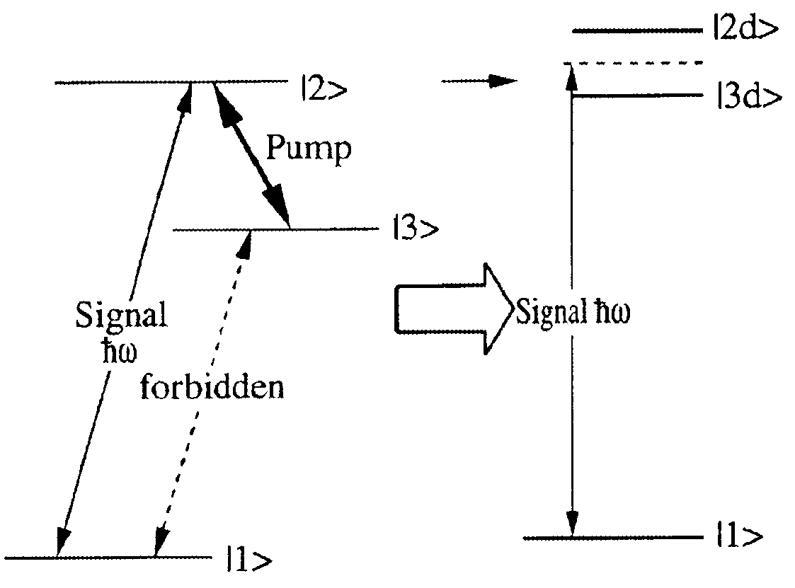
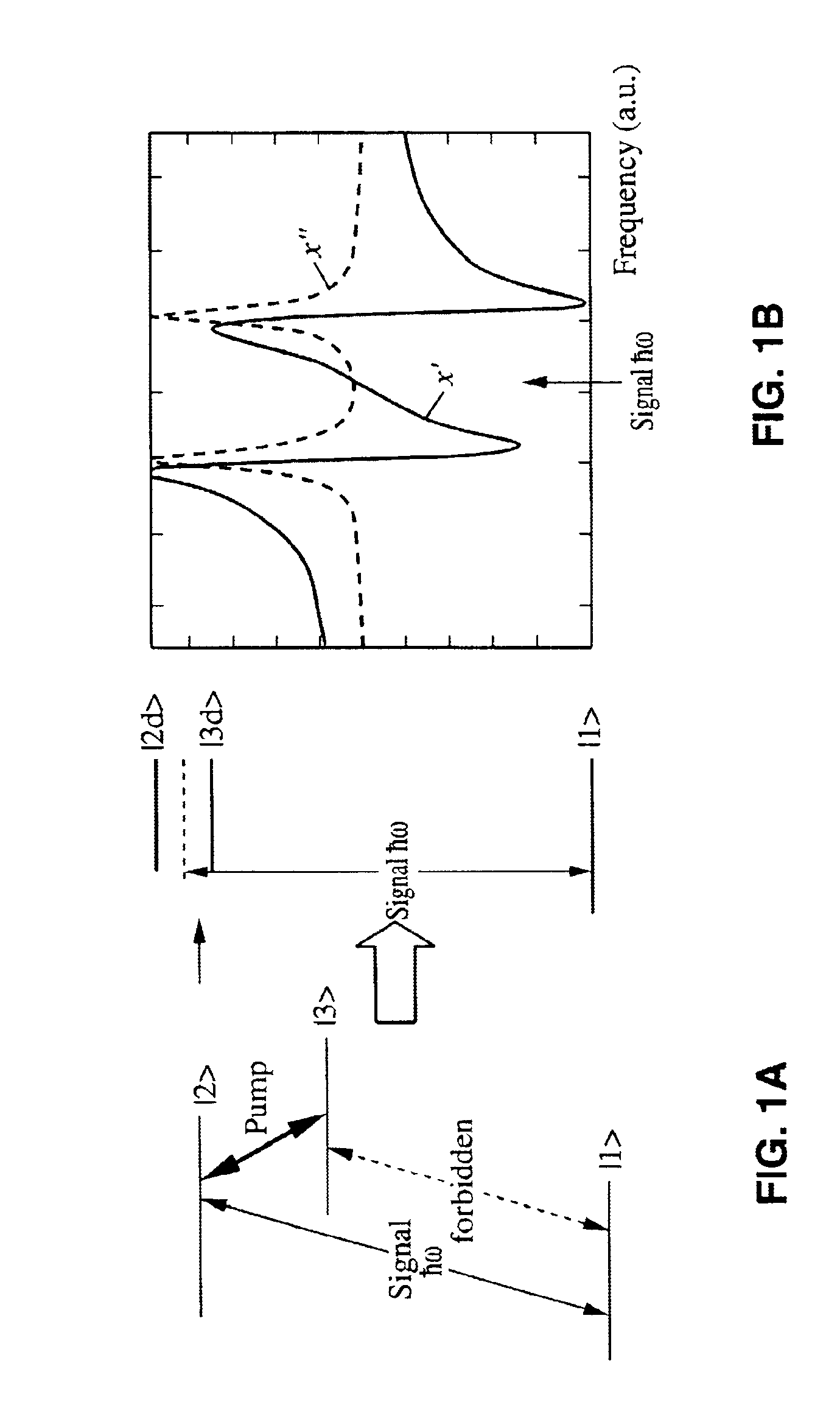
[0158]In this example, disk-shaped QDs are used. |1> is chosen to be the hole level in the valence band; |2> and |3> are chosen to be the electronic levels in the conduction band. In our calculations, ωS=1.55 μm, δ=0, |μ32| / e=25 Å, |μ21| / e=15ξÅ where e and ξ are electron charge and excitonic enhancement factor due to the confinement of electrons and holes inside the QD, respectively. Ten vertically-stacked QD layers with 8 nm diameter, 10 nm height, and surface density of 4×10¹⁰ / cm2 are used. FIG. 13 shows the slow-down factor S and the loss α experienced by the signal light under different pump power intensity. The group velocity slow-down factor (left axis) and the corresponding absorption coefficient (right axis) are plotted as a function of the pump power density. Three different linewidth regimes are compared. Case A, B, C corresponds to 1 μeV, 50 μeV and 1 meV, respectively. Enhancement factor ξ=10 is used in this plot. ℏγ31=ℏγ21 takes the values of 1 μeV, 50 μeV and 1 meV in ...


PUM

PropertyMeasurementUnit
dephasing timeaaaaaaaaaa
lengthaaaaaaaaaa

Abstract

A variable semiconductor all-optical buffer and method of fabrication is provided where buffering is achieved by slowing down the optical signal using a control light source to vary the dispersion characteristic of the medium based on electromagnetically induced transparency (EIT). Photonic bandgap engineering in conjunction with strained quantum wells (QWs) and quantum dots (QDs) achieves room temperature operation of EIT. Photonic crystals are used to sharpen the spectral linewidths in a quantum well structure due to its density of states and in a quantum-dot structure caused by the inhomogeneity of the dot size, typically observed in state-of-the-art QD materials. The configuration facilitates monolithic integration of an optical buffer with an amplifier and control laser to provide advantages over other material systems as candidates for optical buffers.

Description

CROSS-REFERENCE TO RELATED APPLICATIONS[0001]This application claims priority from U.S. provisional application Ser. No. 60 / 324,201 filed on Sep. 21, 2001, incorporated herein by reference.STATEMENT REGARDING FEDERALLY SPONSORED RESEARCH OR DEVELOPMENT[0002]Not ApplicableREFERENCE TO A COMPUTER PROGRAM APPENDIX[0003]Not ApplicableBACKGROUND OF THE INVENTION[0004]A. Field of the Invention[0005]The present invention pertains generally to optical communications, and more particularly to a variable semiconductor all-optical buffer where electromagnetically induced transparency is used to slow light.[0006]B. Publications Incorporated by Reference[0007]The following publications are hereby incorporated by reference:[0008]1. C. J. Chang-Hasnain, et. al. “Integrated external cavity quantum well laser array using single epitaxial growth on a patterned substrate”, Appl. Phys. Lett., vol. 56, No. 5, p. 429, January 1990.[0009]2. C. S. Chang, S. L. Chuang, J. Minch, Y. K. Chen, and T. Tanbun-Ek...

Claims


Application Information

Patent Timeline
Patent Type & Authority Patents(United States)
IPC IPC(8): G02F1/35H01S5/50H01S5/00H01S5/026H01S5/34H01S5/10
CPCB82Y20/00G02F1/35H01S5/50H01S5/026G02F2202/32H01S5/105H01S5/3412H01S5/0057G11C13/04H01S5/11
Inventor CHANG-HASNAIN, CONNIE J.KU, PEI-CHENG
Owner RGT UNIV OF CALIFORNIA
Why Eureka
Try Eureka