Plasma processing apparatus and plasma processing method

a plasma processing and plasma technology, applied in electrical equipment, electrical discharge tubes, decorative arts, etc., can solve the problems of difficult difficult to increase the selectivity of an oxide film to a base material, difficult to stably discharge under a pressure condition below 10 pa, etc., to improve the selectivity of plasma processing, and control the temperature of the sample.

Inactive Publication Date: 2005-06-07
HITACHI LTD
View PDF56 Cites 30 Cited by
  • Summary
  • Abstract
  • Description
  • Claims
  • Application Information

AI Technical Summary

Benefits of technology

[0027]An object of the present invention is to provide a plasma processing apparatus and a plasma processing method capable of easily performing precise manufacturing of a fine pattern on a large sized sample having a diameter of 300 mm or more by obtaining a large-sized and uniform plasma in which dissociation of the processing gas does not excessively progress.
[0028]Another object of the present invention is to provide a plasma processing apparatus and a plasma processing method capable of performing uniform and high-speed processing, and particularly oxide film processing, all over the surface of a large diameter sample.
[0029]A further object of the present invention is to provide a plasma processing apparatus and a plasma processing method capable of improving the selectivity of the etching material of insulator films such as SiO2, SiN, BPSG and the like to the base material.

Problems solved by technology

In a case where a film of the oxide film group is etched using a gas of fluorocarbons, when either of the methods of the ECR described in the above item (1) or the ICP described in the item (2) is employed, it is difficult to increase selectivity of an oxide-film to a base material, for example, Si or SiN since dissociation of the gas progresses excessively.
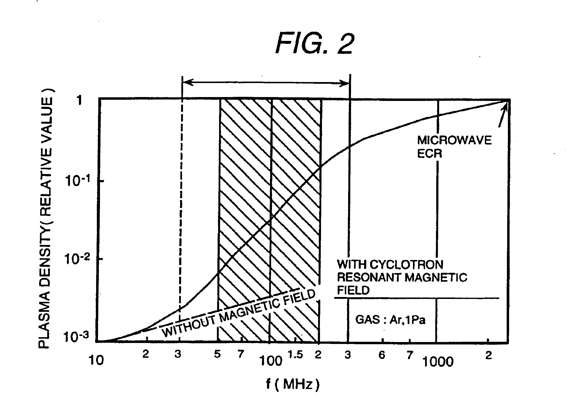
On the other hand, in a conventional method of generating a plasma by applying an RF frequency voltage between a pair of parallel flat plates, it is difficult to stably discharge under a pressure condition below 10 Pa.
However, as a pattern dimension becomes as small as nearly 0.2 μm or smaller, verticality in a processed shape is strongly required and consequently it is inevitable that the gas pressure decreases.
However, in the two-frequency exciting method or the M-RIE method described above, it is difficult to stably produce a plasma having a desired density higher than nearly 5×1010 cm−3 under a pressure condition lower than 4 Pa (0.4 to 4 Pa).
Therefore, it is difficult to produce a plasma having a desired density higher than nearly 5×1010 cm−3 under a pressure condition of 0.4 to 4 Pa.
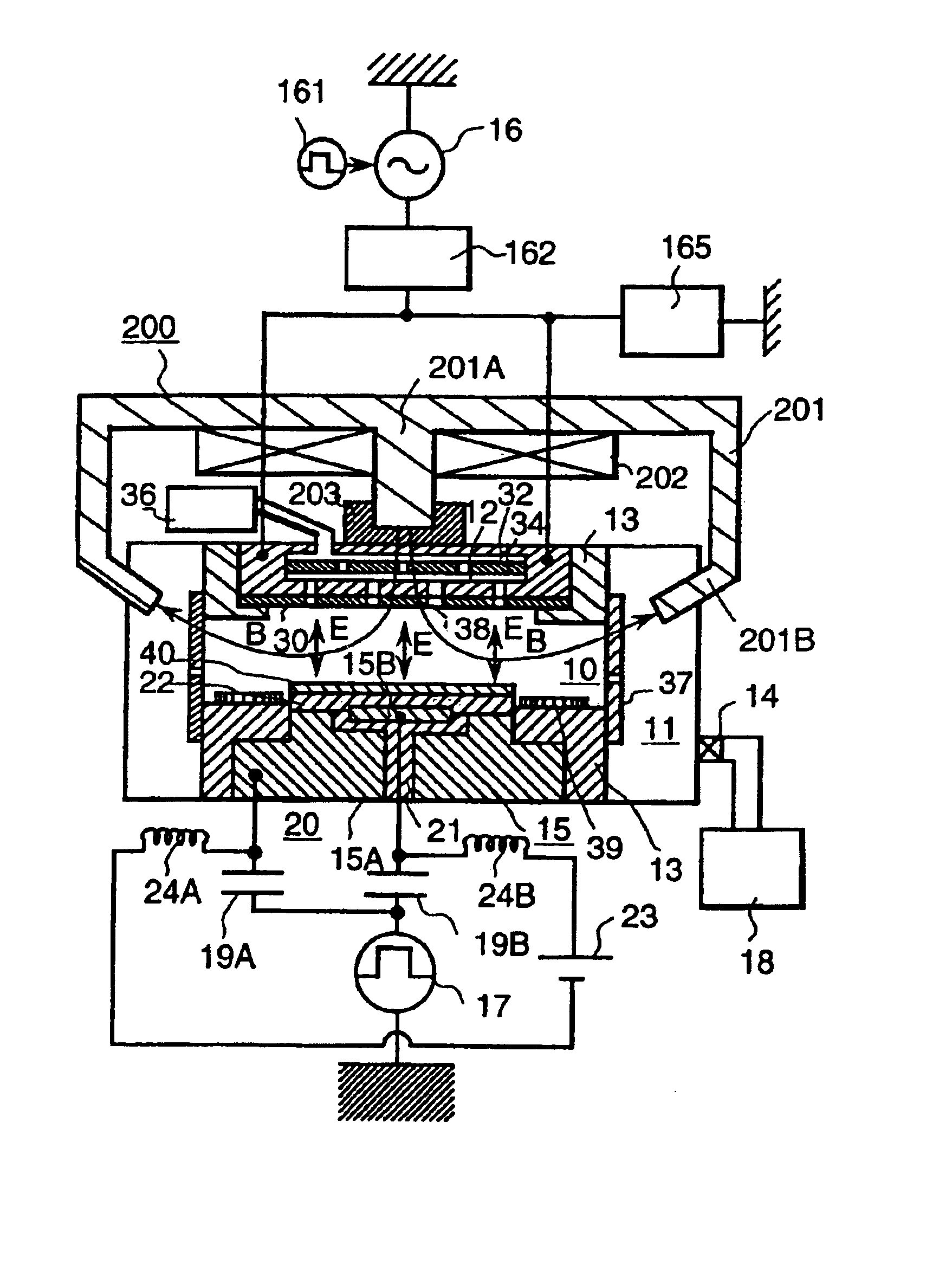
However, there is a disadvantage in that an inclination of the plasma density generally occurs over the surface of the sample due to drift of E×B.
However, there is a disadvantage with this method in that it is difficult to follow a change in a processing condition since a condition for maintaining the plasma uniform is limited to a specified narrow range once the distribution of magnetic field intensity is fixed.
In order to avoid this pressure difference, the gap between the sample table and the opposite electrode must be set to 30 mm or more since, otherwise, the difficulty is likely to be increased.
As described above, in the two-frequency exciting method and the M-RIE method, it is difficult to obtain a uniform plasma density of 5×1010 cm−3 over the surface of a sample having a diameter of 300 mm or more under a pressure condition as low as 0.4 to 4 Pa.
Therefore, in the two-frequency exciting method and the M-RIE method, it is difficult to manufacture the fine pattern of 0.2 μm or smaller on a wafer having a diameter larger than 300 mm uniformly and quickly with a high selectivity of the etching material to the base material.
However, this method has a disadvantage in that in a case where a silicon oxide film or a silicon nitride film is etched using a gas containing fluorine and carbon, it is difficult to attain a desired selectivity to the base material such as Si or the like since dissociation of the gas progresses excessively and a large amount of fluorine atoms and / or molecules and / or fluorine ions are generated.
The ICP method using an electromagnetic field induced by an RF power source also has a disadvantage in that dissociation of the gas progresses excessively, the same as in the ECR method described above.
In such a case, there is a disadvantage in that the plasma density is higher in the central portion of the sample and lower in the peripheral portion of the sample, and accordingly uniformity in the processing all over the surface of the sample is degraded.
However, there is another disadvantage in that reaction products attach onto the bank which becomes a particle producing source to decrease the product yield.
That is, there is a disadvantage in that the processing speed is decreased when one tries to prevent damage of the sample, and the problem of damage arises when one tries to increase the processing speed.
Therefore, there is a disadvantage in that it is difficult to control the energy of the incident ions independently to the plasma density.
Therefore, the pulse bias power source method has a disadvantage in that it cannot cope with a required fine pattern processing while temperature of the sample is properly being controlled.
Further, in the conventional sinusoidal wave output bias power source method disclosed in the specification of U.S. Pat. No. 5,320,982, there is a disadvantage in that an impedance of the sheath portion approaches an impedance of the plasma itself or lower when the frequency becomes high.
If this occurs, an unnecessary plasma is generated near the sheath in the vicinity of the sample by the bias power source, and accordingly the ions are not effectively accelerated and the distribution of the plasma is also degraded to lose controllability of ion energy by the bias power source.
Therefore, as the processing of the sample becomes very small, it becomes clear that there is a limit in the control of the amount of ions, the amount of radicals and the kinds of radicals.
Therefore, the construction cannot use reaction on the surfaces of opposite electrodes effectively, and consequently it is difficult to obtain a high selectivity in this construction.

Method used


Image

  • Plasma processing apparatus and plasma processing method
  • Plasma processing apparatus and plasma processing method
  • Plasma processing apparatus and plasma processing method

Examples


Embodiment Construction

[0098]Embodiments of the present invention will be described below. FIG. 1 shows a first embodiment of a plasma etching apparatus using opposed electrodes to which the present invention is applied.

[0099]Referring to FIG. 1, a processing chamber 10 of a vacuum container has a pair of opposed electrodes composed of an upper electrode 12 and a lower electrode 15. On the lower electrode 15 a sample 40 is mounted. The distance of a gap between the electrodes 12 and 15 is preferably not smaller than 30 mm in order to suppress a pressure difference on the sample to within 10% when the sample has a large diameter of about 300 mm or larger. In order to decrease amounts of fluorine atoms, molecules and ions, the distance is desired to be not larger than 100 mm, preferably, not larger than 60 mm from the view point of effectively using a reaction product on the surfaces of the upper and the lower electrodes. A high frequency electric power source 16 for supplying a high frequency energy is con...


PUM

PropertyMeasurementUnit
diameteraaaaaaaaaa
frequencyaaaaaaaaaa
magnetic fieldaaaaaaaaaa

Abstract

A method of plasma-processing is provided which includes placing a sample on one of electrodes provided in a vacuum processing chamber and holding the sample onto the electrodes by an electrostatic attracting force. A processing gas is introduced into an environment in which said sample is placed, and the environment is evacuated to a pressure condition for processing said sample. The processing gas is then formed into a plasma under the pressure condition, the sample is processed by the plasma, and a pulse bias voltage having a pulse cycle of 0.1 μm to 10 μm is applied to the sample.

Description

CROSS-REFERENCE TO RELATED APPLICATION[0001]This application is a divisional of application Ser. No. 08 / 808,805, now U.S. Pat. No. 6,129,806 filed on February 28, 1997, the entire disclosure of which is hereby incorporated by reference.BACKGROUND OF THE INVENTION[0002]The present invention relates to a plasma processing apparatus and a plasma processing method, and more particularly relates to a plasma processing apparatus and a plasma processing method suitable for forming a fine pattern in a semiconductor device manufacturing process.[0003]The need for improving the fine pattern manufacturing capability and the processing speed in plasma processing is growing further as integration of semiconductor devices become higher. In order to respond to this need, it is required to decrease the pressure of the processing gas and to increase the plasma density.[0004]In regard to plasma processing apparatuses aiming to decrease the pressure of the processing gas and to increase the plasma den...

Claims


Application Information

Patent Timeline
Patent Type & Authority Patents(United States)
IPC IPC(8): H01J37/32H01L21/00
CPCH01J37/32082H01L21/67069H01J37/32678H01J37/32623
Inventor KAJI, TETSUNORITACHI, SHINICHIOTSUBO, TORUWATANABE, KATSUYAMITANI, KATSUHIKOTANAKA, JUNICHI
Owner HITACHI LTD
Why Eureka
Try Eureka