Sloped via contacts

a technology of contact vias and contacts, which is applied in the direction of semiconductor devices, semiconductor/solid-state device details, electrical devices, etc., can solve the problem of low signal loss from the device to the external circuit, and achieve the effect of reducing the overall chip area, low signal loss, and high chip density on the wafer

Inactive Publication Date: 2005-06-07
AVAGO TECH WIRELESS IP SINGAPORE PTE
View PDF5 Cites 79 Cited by
  • Summary
  • Abstract
  • Description
  • Claims
  • Application Information

AI Technical Summary

Benefits of technology

[0007]By using a sloped via contact rather than a bonded wire, a signal from a device on the front of the chip can take a much shorter path to the external circuitry. For high frequency applications, this results in very low signal losses from the device to the external circuit leads. Additionally, since the contact pads at the ...

Problems solved by technology

For high frequency applications, this results in very lo...

Method used


Image

  • Sloped via contacts
  • Sloped via contacts
  • Sloped via contacts

Examples


Embodiment Construction

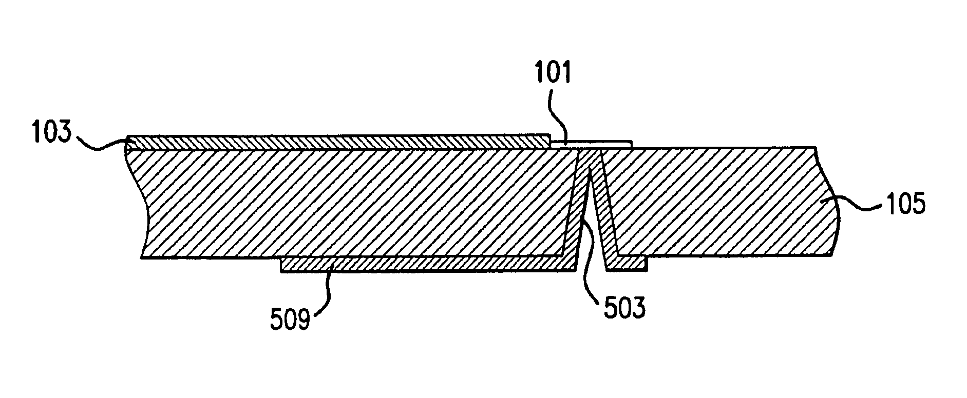
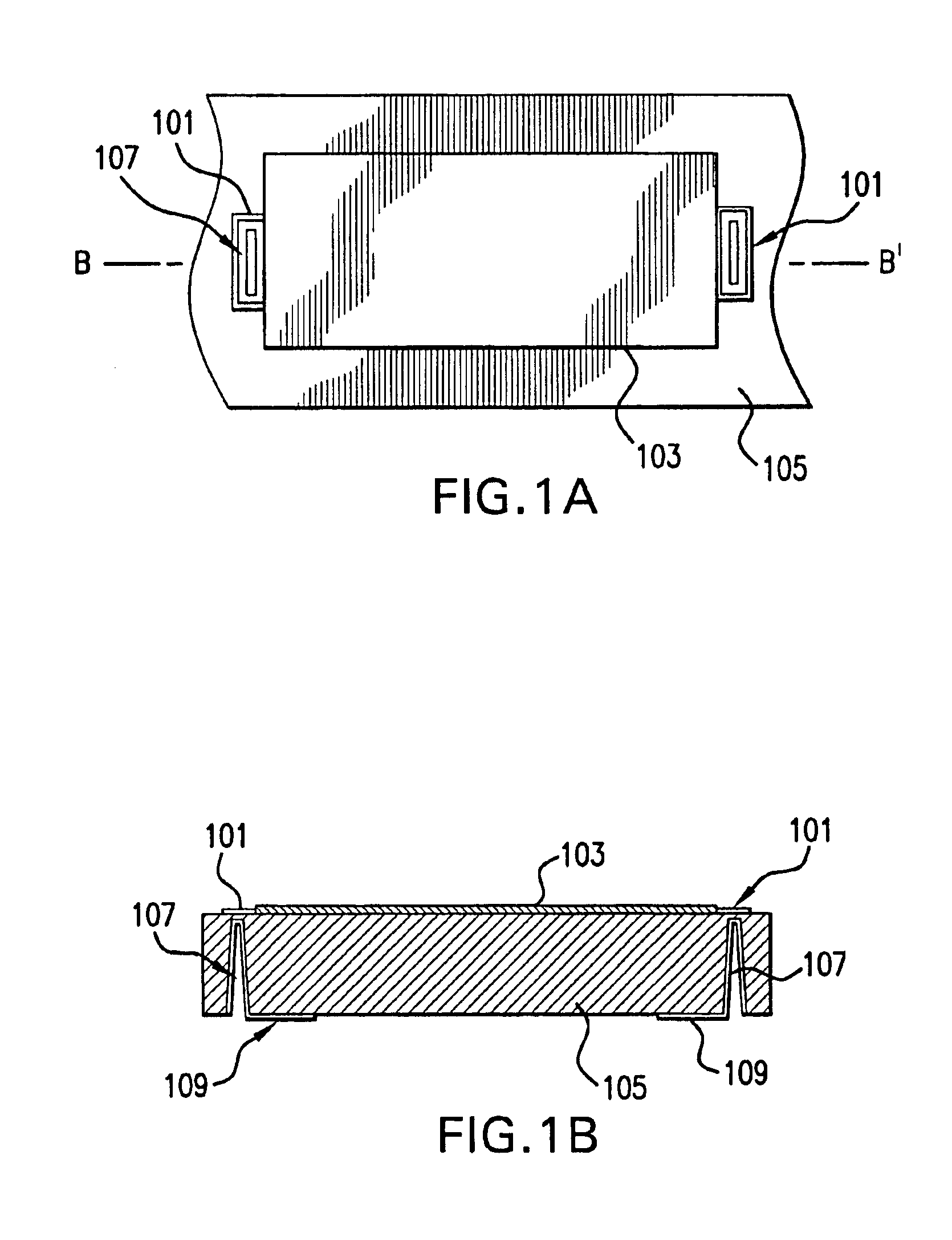
[0016]FIG. 1A shows a top view of a preferred embodiment of a wafer section having sloped via contacts made in accordance with the teachings of the present invention. Contacts 101 are connected to a device 103 on the front of a wafer 105. The opening of a sloped via contact 107 is located within each contact 101. Although contacts 101 and sloped via contacts 107 are shown with a rectangular shape, contacts 101 and sloped via contacts 107 can be circular, square, oval, or any other shape. Additionally, although each sloped via contact 107 is shown centered within a contact 101, sloped via contact 107 can be positioned anywhere within contact 101 as long as an electrical connection is made between them, and no interference occurs with connections to external circuitry.

[0017]FIG. 1B shows a cross-sectional view of the wafer section of FIG. 1A, taken along the line B-B′ in FIG. 1A. Sloped via contacts 107 gradually increase in width from front to back of wafer 105, so that each sloped v...


PUM


Abstract

A sloped via contact is used to connect a contact on the front side of a wafer to a contact on the back side of the wafer. The walls of a small (less than 50-80 microns wide) via have typically been difficult to coat with metal. The present invention forms a small via with sloped walls, allowing easy access to the inside walls of the via for metal sputtering or plating. The small via can be formed using a dry etch process such as the well-known deep reactive ion etching (DRIE) process. Using any isotropic plasma etch process, the walls of the via are further etched from the wafer backside to create sloped walls in the via. The via is then coated with metal to make it conductive.

Description

[0001]This is a Divisional of copending application Ser. No. 10 / 029,193, filed on Dec. 20, 2001, the entire disclosure of which is incorporated herein by reference.FIELD OF THE INVENTION[0002]The invention is directed towards semiconductor wafer manufacturing and more specifically, towards contact vias in semiconductor wafers.BACKGROUND OF THE INVENTION[0003]Semiconductor chips are often electrically connected to external circuitry using wire bonds. Wires are connected between contact pads on the chip surface and the desired external circuitry. However, the wire length adds unwanted resistance and inductance to the system, which can negatively affect the performance of the chip. This is especially true of chips designed for use at higher frequencies. Furthermore, the contact pads on the chip surface increase the area of each chip, which decreases the number of chips that can be manufactured on a single wafer. Wire bonding is also an expensive and time-consuming assembly process.[000...

Claims


Application Information

Patent Timeline
IPC IPC(8): H01L21/70H01L23/48H01L21/768
CPCH01L21/76898H01L23/481H01L2924/09701H01L2224/05548H01L2224/02372H01L2224/0401Y10S438/928
Inventor GEEFAY, FRANK SGAN, QING
Owner AVAGO TECH WIRELESS IP SINGAPORE PTE
Why Eureka
Try Eureka