Method and apparatus for determining endpoint of semiconductor element fabricating process

a technology of semiconductor elements and endpoints, which is applied in the direction of semiconductor/solid-state device testing/measurement, instruments, electric discharge tubes, etc., can solve the problems of low reproducibility in terms of thickness, the inability of time monitor techniques to accurately measure the actual final thickness of the siosub>2 /sub>layer remaining on the silicon substrate, and the inability of endpoint determining units to reliably determine the endpoint of the etching process based on the sampl

Inactive Publication Date: 2005-06-07
HITACHI LTD
View PDF31 Cites 33 Cited by
  • Summary
  • Abstract
  • Description
  • Claims
  • Application Information

AI Technical Summary

Benefits of technology

[0021]It is an object of the present invention to provide a method and apparatus for determining an endpoint of semiconductor device manufacturing process and a method and apparatus for processing a material by using the endpoint determining method and apparatus, which can solve the above-described problems experienced with the conventional techniques.
[0035]Further, it is also possible to provide an etching process that can control online the etch quantity of each layer of semiconductor devices to a desired value with high precision. It is also possible to provide an etch depth and thickness measuring apparatus that can precisely measure online the actual etch quantity of a layer being processed.

Problems solved by technology

As a result, a level of signal sampled from the photodetector becomes small, making it difficult for an endpoint determining unit to determine the etching process endpoint reliably based on the sampled signal from the photodetector.
An actual layer, for example, an SiO2 layer formed by the LPCVD (low pressure chemical vapor deposition) technique, however, is known to have a low reproducibility in terms of thickness.
Hence, the time monitor technique cannot precisely measure the actual final thickness of the SiO2 layer remaining on a silicon substrate.
In some cases the etching may inadvertently stop while in process.
The conventional method, however, monitors only the time in determining the etching process endpoint and does not provide an appropriate means of dealing with variations over time of the etch rate.
These requirements are not met satisfactorily.
Another problem is that an etched area of the insulating film is in many cases less than 1%, which means that a change in intensity of plasma-induced light emitted from a reactive product created during etching is small.
Hence an endpoint determining system capable of detecting even very small changes is required, but no practical and inexpensive systems with such a capability are available.

Method used


Image

  • Method and apparatus for determining endpoint of semiconductor element fabricating process
  • Method and apparatus for determining endpoint of semiconductor element fabricating process
  • Method and apparatus for determining endpoint of semiconductor element fabricating process

Examples


first embodiment

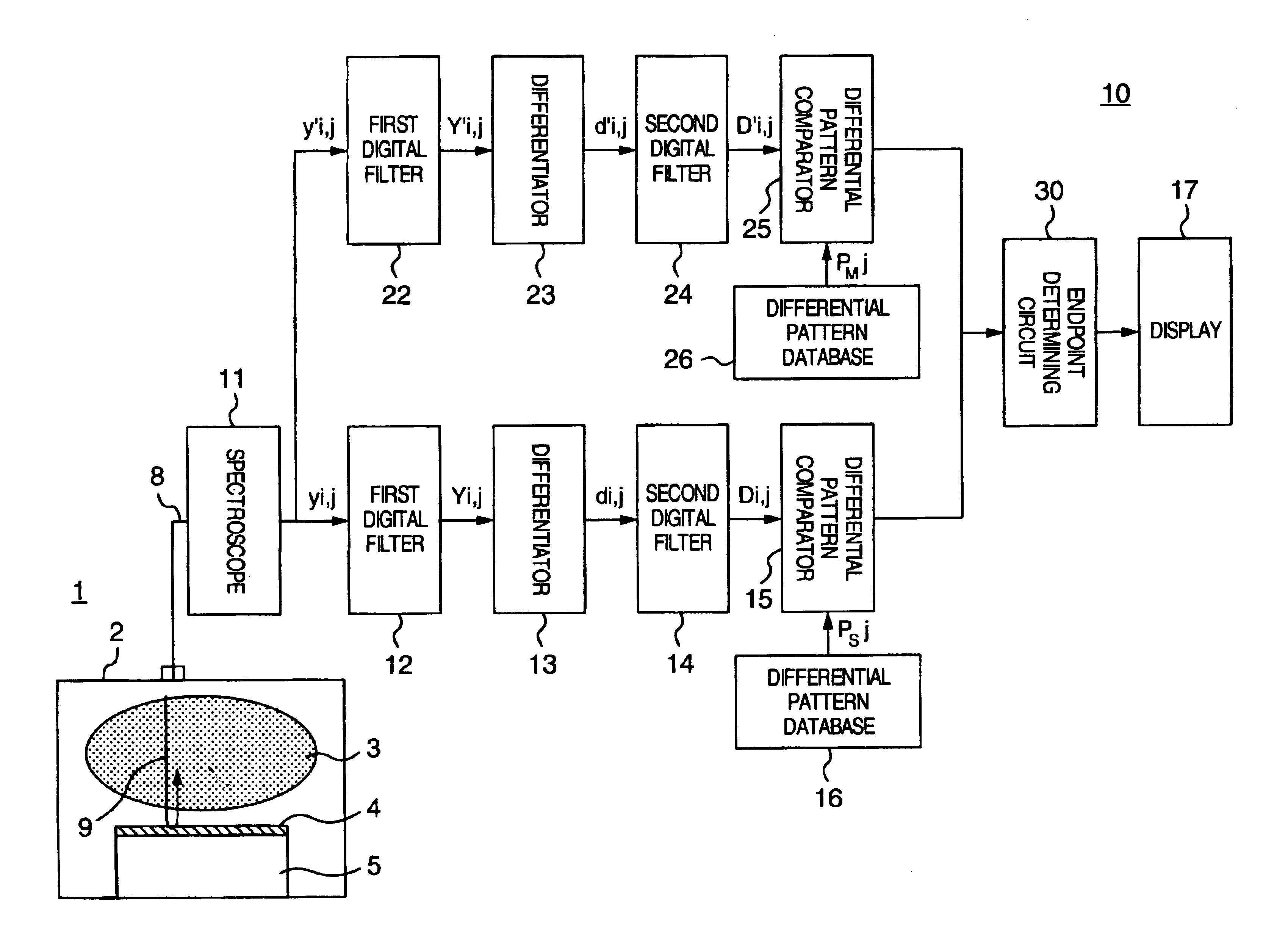
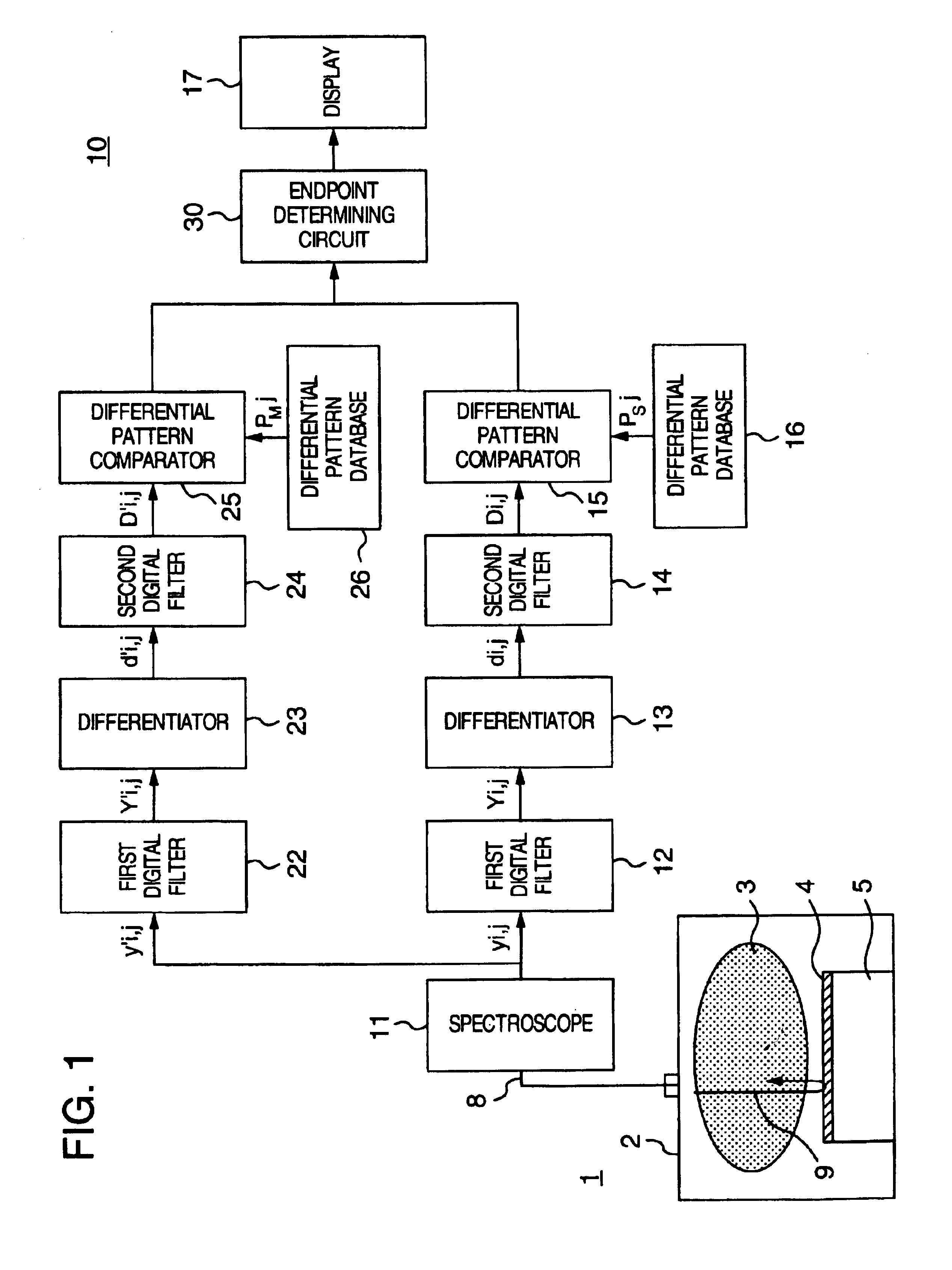
[0054]Embodiments of the present invention will be described. In the following embodiments, constitutional members with similar functions to those of the first embodiment carry like reference numbers and their detailed descriptions are omitted. As the endpoint determining method used in the semiconductor device manufacturing process according to the present invention, we will describe a method of measuring an etch quantity (etched depth and film thickness) in a wafer etching process. It should be noted that the present invention is not limited to this method and can also be applied to a method of measuring an amount of deposition (deposited film thickness) or the like in such film deposition processes as plasma CVD and sputtering.

[0055]Now, a first embodiment of the present invention will be described by referring to FIG. 1 to FIG. 4.

[0056]In this embodiment, when plasma etching is to be performed on a material to be processed such as a semiconductor wafer, standard patterns PS and ...

second embodiment

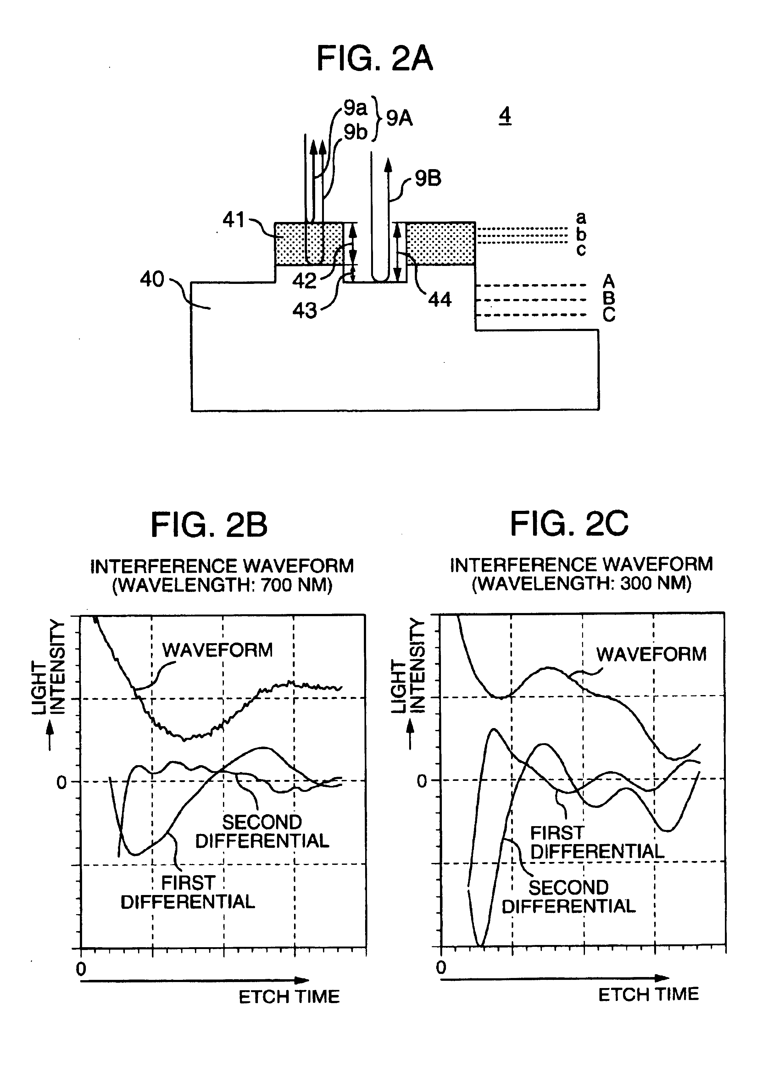
[0090]Next, the present invention will be described by referring to FIGS. 8, 9, 10 and 11. The configuration of this embodiment shown in FIG. 8 is identical with the configuration 11-19 of FIG. 5 for one wavelength band and the operation of the endpoint determining circuit 130 is different from that of the endpoint determining circuit 30 of FIG. 5. The structure of the material to be etched is shown in FIG. 9. The area of a polysilicon 50 processed by this etching process lies where there is no mask layer 51 (e.g., nitride film and photoresist). The observed interference light is produced by the interference between light 90A reflected by the surface of the polysilicon 50 and light 90B reflected by an underlying oxide film 52. A method of measuring the etch quantity (remaining thickness 53: thickness of polysilicon measured from the underlying oxide film) by measuring the interference light will be explained with reference to the flow chart of FIG. 10.

[0091]First, a target remaining...

third embodiment

[0098]Next, the present invention will be described by referring to FIG. 12 and FIG. 13. In controlling the etch depth, this embodiment determines the etch depth from the initial film thickness and the measured remaining film thickness because wafers have errors in the thickness of an organic film. The configuration shown in FIG. 12 is the same as the configuration 11-19 of FIG. 8 and the operation of the endpoint determining circuit 230 differs from that of the endpoint determining circuit 130 of FIG. 8. The structure of a material to be etched is shown in FIG. 13. The area of an organic film 60 to be etched (groove structure) lies where there is no mask layer 61 (e.g., nitride film and photoresist). The interference light observed is produced by interference between light reflected by the surface of the organic film and light reflected by an interconnect layer 62 (e.g., Cu).

[0099]The method of measuring an etch quantity (groove depth 65: distance between D and E) by measuring the ...


PUM


Abstract

Standard patterns of differential values of interference light that correspond to a predetermined step height of the first material being processed and standard patterns of differential values of interference light that correspond to a predetermined remaining mask layer thickness of the material are set. These standard patterns use wavelengths as parameters. Then, the intensities of interference light of multiple wavelengths are measured for a second material that has the same structure as the first material. Actual patterns with wavelength as parameter are determined from differential values of the measured interference light intensities. Based on the standard patterns and the actual patterns of the differential values, the step height and the remaining mask layer thickness of the second material are determined.

Description

CROSS-REFERENCE TO RELATED APPLICATION[0001]The present invention is related to U.S. patent application Ser. No. 09 / 793,624 filed Feb. 27, 2001.BACKGROUND OF THE INVENTION[0002]The present invention relates to a method and apparatus which processes a material by using a method and apparatus for determining an endpoint of a semiconductor device manufacturing process. More specifically, the present invention relates to a method and apparatus for determining an endpoint of semiconductor device manufacturing process and a method and apparatus for processing a material by using the endpoint determining method and apparatus, which detects an etch quantity of, or deposition on, a material being processed in a semiconductor integrated circuit manufacturing process. More specifically, the present invention relates to a method and apparatus for measuring an etch depth and a thickness of a material being processed and a method and apparatus for processing a material by using the etch depth / thi...

Claims


Application Information

Patent Timeline
Patent Type & Authority Patents(United States)
IPC IPC(8): G01B11/06
CPCG01B11/0675H01L22/26H01J37/32963
Inventor USUI, TATEHITOFUJII, TAKASHIYOSHIGAI, MOTOHIKOKAJI, TETSUNORIYAMAMOTO, HIDEYUKI
Owner HITACHI LTD
Why Eureka
Try Eureka