Methods of forming tungsten nucleation layer

a nucleation layer and tungsten technology, applied in the direction of polycrystalline material growth, crystal growth process, chemically reactive gas, etc., can solve the problems of high directional bombardment, uneven nucleation, and relative difficulty in getting tungsten to deposit on the substrate, so as to eliminate the nucleation delay

Inactive Publication Date: 2005-06-14
NOVELLUS SYSTEMS
View PDF3 Cites 55 Cited by
  • Summary
  • Abstract
  • Description
  • Claims
  • Application Information

AI Technical Summary

Benefits of technology

[0008]According to another aspect of this invention, the substrate is exposed to a boron hydride-containing gas, such as B2H6, before the tungsten nucleation layer is formed. The boron hydride pretreatment renders the surface of the substrate highly active and in many cases this essentially eliminates the nucleation delay. The boron hydride pretreatment is effective on a wide variety of surfaces, including, for example, silicon, silicon dioxide, silicon nitride and titanium nitride.

Problems solved by technology

One problem with tungsten, however, is that it is relatively difficult to get tungsten to start depositing on a substrate (e.g., a semiconductor wafer or oxide layer).
A disadvantage of this technique is that the ion bombardment is highly directional in nature and tends to be directed primarily at flat horizontal surfaces rather than vertical surfaces such as the sidewalls of a trench or via.
The nucleation layer thus begins preferentially on the flat horizontal surfaces, with the result that the nucleation is uneven and the step coverage is poor.

Method used


Image

  • Methods of forming tungsten nucleation layer
  • Methods of forming tungsten nucleation layer
  • Methods of forming tungsten nucleation layer

Examples


Embodiment Construction

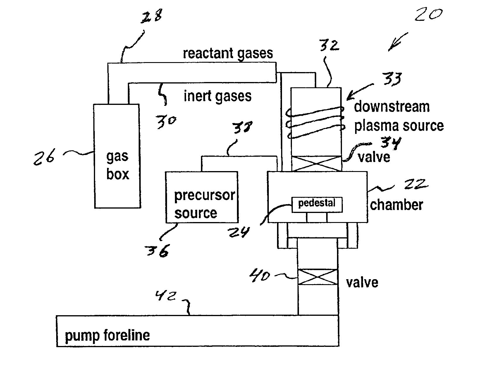
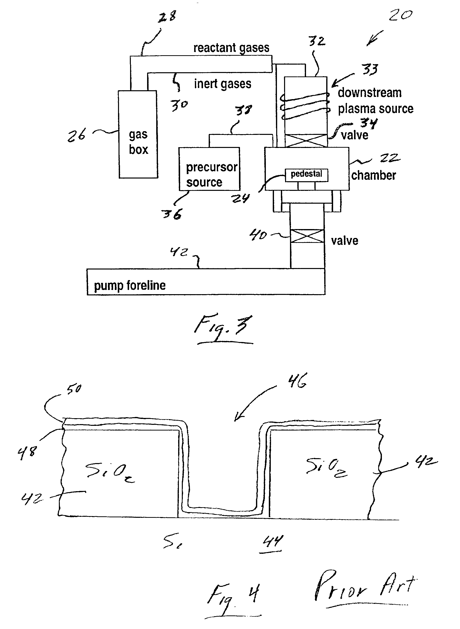
[0021]FIG. 3 is a schematic diagram of a chemical vapor deposition (CVD) reactor 20 in which the method of this invention can be performed. CVD reactor 20 includes a reaction chamber 22 in which a pedestal 24 for holding a semiconductor wafer or other substrate is contained. Reactant gases and inert gases are fed into chamber 22 from a gas box 26 through gas lines 28 and 30, which connect to a downstream plasma source 32. Downstream plasma source 32 is connected to chamber 22 via a valve 34. A tungsten-containing gas such as tungsten hexafluoride (WF6) originates from a precursor source 36, which connects to chamber 22 via a line 38.

[0022]Downstream from chamber 22 is a valve 40, which leads to a pump foreline 42. An exhaust pump (not shown) connected to pump foreline 42 is used to remove gases from chamber 22.

[0023]In the process of this invention, a semiconductor wafer or other substrate is placed on pedestal 24. The pressure in reaction chamber 22 is set at 0.3-40 Torr and temper...


PUM

PropertyMeasurementUnit
temperatureaaaaaaaaaa
pressureaaaaaaaaaa
temperatureaaaaaaaaaa

Abstract

The nucleation delay in the formation of a tungsten layer on a substrate is reduced or eliminated by alternative processes. In one process the substrate is exposed to atomic hydrogen before the tungsten nucleation layer is formed. In the other process the substrate is exposed to a boron hydride such as diborane (B2H6) before the nucleation layer is formed. The process works effectively to reduce or eliminate the tungsten nucleation delay on a variety of surfaces, including silicon, silicon dioxide, silicon nitride and titanium nitride.

Description

FIELD OF THE INVENTION[0001]This invention relates to methods of depositing a tungsten layer in the fabrication of integrated circuits and, in particular, methods of forming a tungsten nucleation layer.BACKGROUND OF THE INVENTION[0002]Tungsten is used to form conductive lines in integrated circuit (IC) devices. Because the resistivity of tungsten is higher than the resistivity of aluminum or copper, the use of tungsten has generally been relegated to filling vertical features such as vias and trenches and local interconnects. Tungsten has an advantage over aluminum and copper in that tungsten does not tend to migrate into and contaminate the silicon or dielectric layers of the device. Copper in particular is highly contaminating and barrier layers must be provided to prevent the copper from contaminating the silicon and dielectric layers. Moreover, aluminum and copper must be sputtered or electroplated onto the substrate, whereas tungsten can be deposited by chemical vapor depositio...

Claims


Application Information

Patent Timeline
Patent Type & Authority Patents(United States)
IPC IPC(8): C30B25/14C23C16/02C23C16/14C23C16/455
CPCC23C16/0218C23C16/45525C23C16/14
Inventor FAIR, JAMES A.TAYLOR, NERISSASUNG, JUNGHWAN
Owner NOVELLUS SYSTEMS
Why Eureka
Try Eureka