Oscillation circuit and a communication semiconductor integrated circuit

a technology of oscillating circuit and integrated circuit, which is applied in the direction of pulse generator, pulse technique, modulation, etc., can solve the problems of inability to measure the output amplitude the measurement method described above for measuring the frequency of the divided signal, and the lc resonance vco to stop oscillating, so as to reduce the parasitic capacitance, narrow down the variable frequency range, and widen the variable frequency range

Inactive Publication Date: 2005-06-14
EPOCH MICROELECTRONICS +1
View PDF2 Cites 74 Cited by
  • Summary
  • Abstract
  • Description
  • Claims
  • Application Information

AI Technical Summary

Benefits of technology

[0016]Since the substrate voltage switching means can reduce a parasitic capacitance on the drain of the MOS transistor, the oscillation circuit can provide a wider variable frequency range. Particularly, an LC resonance oscillation circuit which is required to oscillate at a high frequency is made up of an inductor having a small inductance and a capacitive element having a small capacitance, so that the parasitic capacitance accounts for a large proportion. Since the parasitic capacitance could narrow down the variable frequency range in applications which require a wide variable frequency range such as an oscillation circuit for communication, the application of the substrate voltage switching means for reducing the parasitic capacitance is extremely effective in such applications.

Problems solved by technology

Also, the output amplitude of the LC resonance VCO depends on a loss in an LC resonance circuit, and an excessively large loss will cause the LC resonance VCO to stop oscillating.
However, the measuring method as described above for measuring the frequency of the divided signal is disadvantageous in the inability to measure the output amplitude of the VCO.
However, if a terminal (pad) was provided for directly measuring the output of the VCO, the terminal would cause an increase in a parasitic capacitance to offset the constants of the LC resonance circuit and accordingly change the characteristics of the VCO, thereby failing to precisely measure the frequency.
When a wide variable frequency is required as is the case with the dual-band system and triple-band system, a large parasitic capacitance would exacerbate a substantial capacitance changing rate, resulting in a failure in providing a desired variable frequency range.

Method used


Image

  • Oscillation circuit and a communication semiconductor integrated circuit
  • Oscillation circuit and a communication semiconductor integrated circuit
  • Oscillation circuit and a communication semiconductor integrated circuit

Examples


Embodiment Construction

[0030]In the following, embodiments of the present invention will be described with reference to the accompanying drawings.

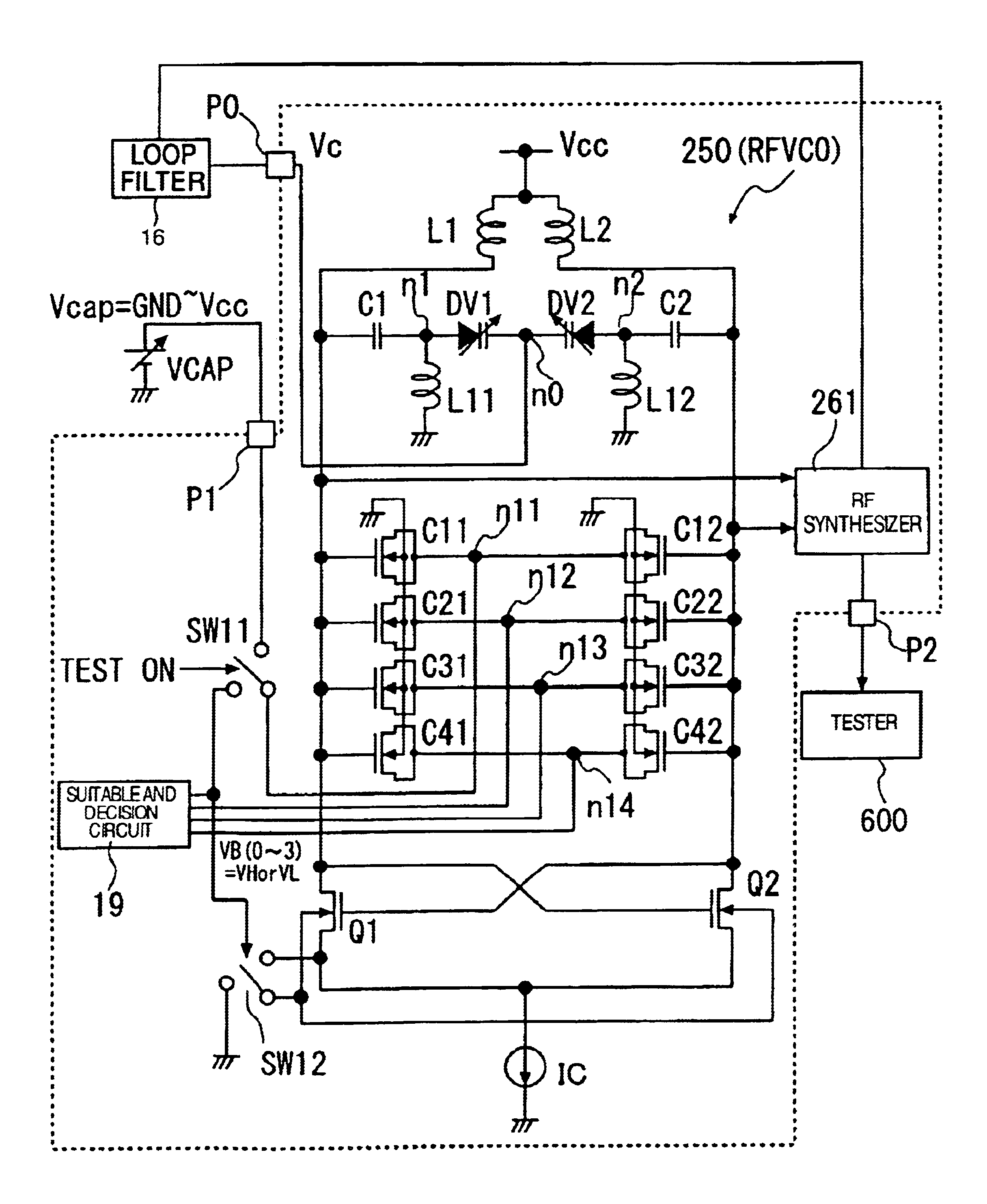
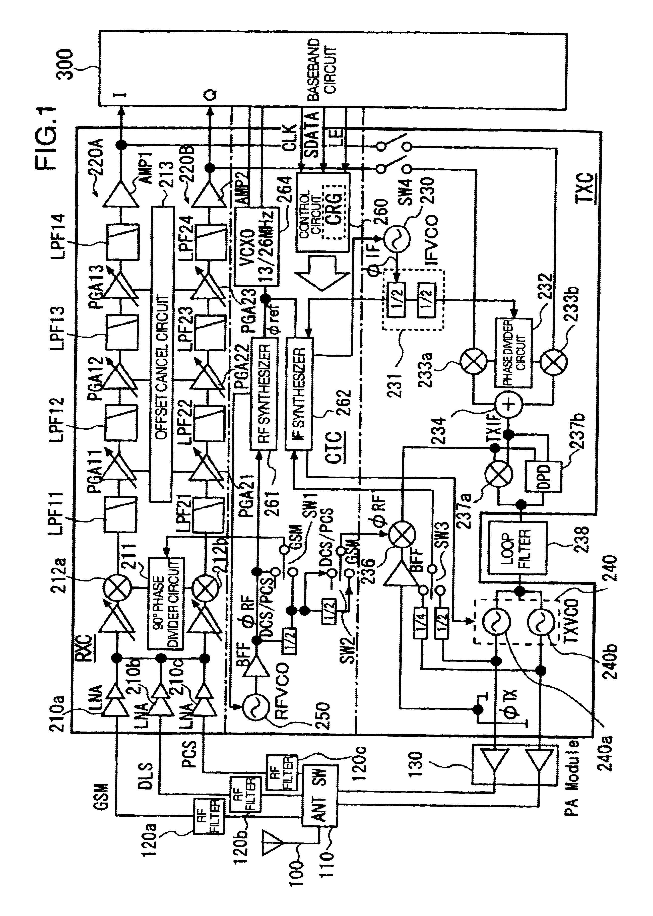
[0031]FIG. 1 is a block diagram illustrating an exemplary configuration of a multi-band communication semiconductor integrated circuit (high frequency IC) to which the present invention is applied, and a radio communication system using the communication semiconductor integrated circuit.

[0032]The radio communication system illustrated in FIG. 1 comprises an antenna 100 for transmitting and receiving signal radio waves; a switch 110 for switching transmission and reception; high frequency filters 120a-120c such as SAW filters for removing unwanted waves from a reception signal; a high frequency power amplifier 130 for amplifying a transmission signal; a high frequency IC 200 for demodulating a reception signal and modulating a transmission signal; and a baseband circuit (LSI) 300 for converting transmission data to I, Q signals and controlling the high frequency ...


PUM


Abstract

A voltage controlled LC resonance oscillation circuit has a plurality of capacitive elements connected to an output node. These capacitive elements are applied with voltages at opposing terminals for selecting an oscillating frequency band, so that the oscillating frequency band can be changed step by step in accordance with the selection voltage. The capacitive elements include at least one variable capacitive element such as a MOS capacitor, the capacitance of which is varied in accordance with a voltage applied thereto. The MOS capacitor is similar in structure to a MOS transistor. The variable capacitive element can be supplied at a terminal opposite to the output node with a voltage from a variable voltage source, for example, in place of the selection voltage. The voltage controlled LC resonance oscillation circuit can measure the output amplitude and oscillating frequency without affecting the characteristics thereof, and reduce the parasitic capacitance.

Description

BACKGROUND OF THE INVENTION[0001]The present invention relates generally to techniques which are effectively applied for improving the characteristics of a voltage controlled oscillation circuit (VCO) capable of switching from one oscillating frequency to another as well as the characteristics of an on-chip VCO, and facilitating measurements of the characteristics of such VCOs, and more particularly, to techniques which are effectively utilized in a VCO mounted in a high frequency semiconductor integrated circuit for demodulating a reception signal and modulating a transmission signal in radio communication apparatuses, for example, a portable telephone and the like which can transmit and receive signals in a plurality of bands.[0002]A radio communication system such as a portable telephone uses a PLL (phase locked loop) circuit which has a VCO for generating an oscillating signal at a predetermined frequency. The oscillating signal is combined with a reception signal and a transmis...

Claims


Application Information

Patent Timeline
Patent Type & Authority Patents(United States)
IPC IPC(8): H03L5/00H03L7/099H03L7/08H03L7/10H01L21/822G01R31/28H01L27/04H03B5/12
CPCH03L5/00H03L7/099H03L7/10H03B5/1228H03B5/1262H03B5/1243H03B5/1253H03B5/1293H03B5/1215H03L7/101
Inventor KITAMURA, TOMOMITSUKIMURA, YASUYUKISUYAMA, KENDEC, ALEKSANDER
Owner EPOCH MICROELECTRONICS
Why Eureka
Try Eureka