HDP-CVD dep/etch/dep process for improved deposition into high aspect ratio features

a technology of high aspect ratio and deposition process, which is applied in the direction of chemical vapor deposition coating, coating, semiconductor devices, etc., can solve the problems of affecting device operation, unable to completely fill the semiconductor, and early dep/etch/dep process known to the inventors were limited to thermal cvd and pecvd processes, so as to achieve superior gapfill capabilities and throughput. high

Inactive Publication Date: 2005-06-21
APPLIED MATERIALS INC
View PDF50 Cites 280 Cited by
  • Summary
  • Abstract
  • Description
  • Claims
  • Application Information

AI Technical Summary

Benefits of technology

[0013]Embodiments of the present invention pertain to an in situ HDP-CVD dep / etch / dep process that overcomes the problems of previously known processes. Embodiments of the invention provide higher throughput than ex situ dep / etch / dep processes and have superior gapfill capabilities as compared to similar non-dep / etch / dep HDP-CVD processes.

Problems solved by technology

Gaps having a combination of a high aspect ratio and a small width present a challenge for semiconductor manufacturers to fill completely.
In short, the challenge usually is to prevent the deposited film from growing in a manner that closes off the gap before it is filled.
Failure to fill the gap completely results in the formation of voids in the deposited layer, which may adversely affect device operation, for example by trapping undesirable impurities.
Most of the early dep / etch / dep processes known to the inventors were limited to thermal CVD and PECVD processes.
It has been found in practice, however, that while HDP-CVD processes generally have better gapfill capabilities than similar non-HDP-CVD processes, for certain gap widths there remains a limit to the aspect ratio of gaps that can be filled.
Such STI applications often provide the most challenging gapfill requirements for insulation layers especially considering that many integrated circuits now use copper and appropriate dual damascene techniques as the interconnect structure.
Such an etch step is a fully directional etch (i.e., an anisotropic sputter etch) that is susceptible to corner clipping problems.
The inventors of the present patent have determined that transitioning from such a fluorine-containing etch step straight to a subsequent deposition step as taught in the '881 patent results in an undesirable amount of fluorine being incorporated at the interface of the first and second layers of the film and may also result in etch defects (silicon-rich pockets on the surface of the etched film that look like particles).
Regardless of how such fluorine is incorporated in the film, the result is generally undesirable.
In other situations, the existence of fluorine in the layer may make a semiconductor manufacturer wary of the integrity of the layer.

Method used


Image

  • HDP-CVD dep/etch/dep process for improved deposition into high aspect ratio features
  • HDP-CVD dep/etch/dep process for improved deposition into high aspect ratio features
  • HDP-CVD dep/etch/dep process for improved deposition into high aspect ratio features

Examples


Embodiment Construction

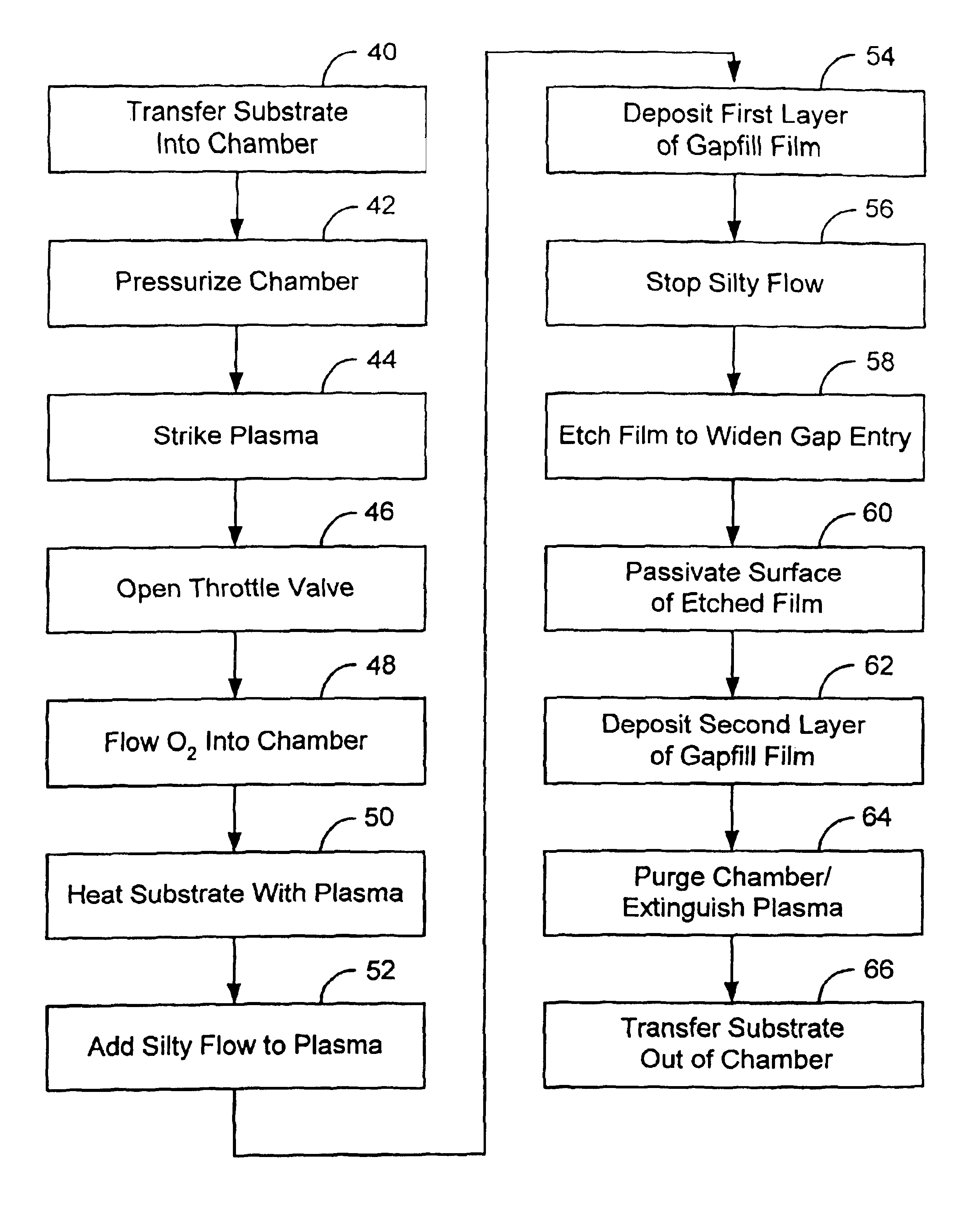
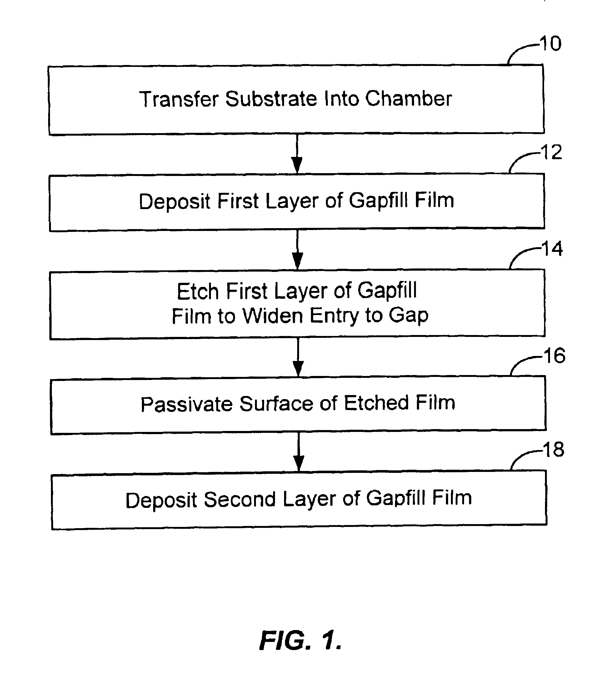
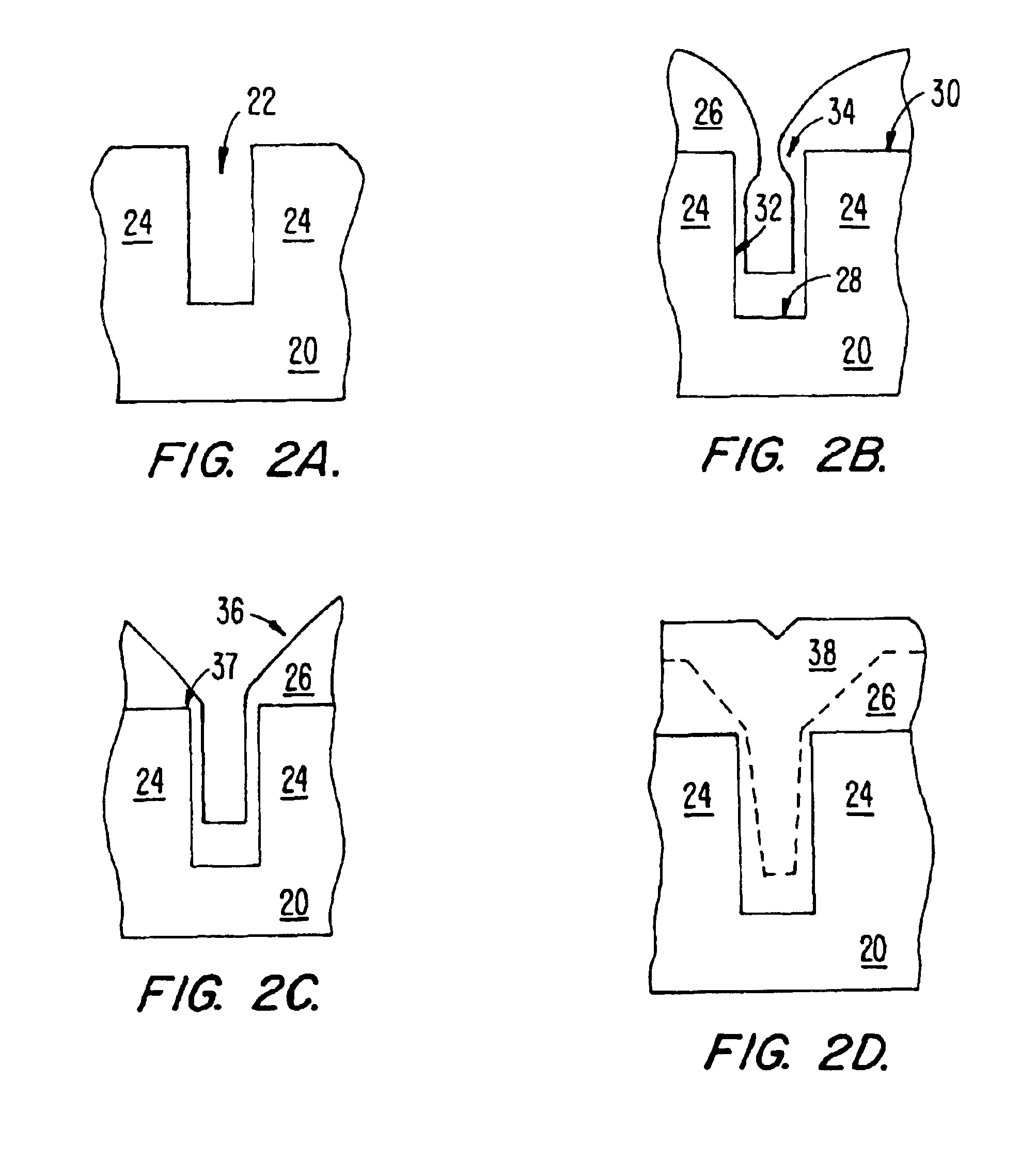
[0024]Embodiments of the invention pertain to a multistep high density plasma process for depositing dielectric material into high aspect ratio features. Embodiments of the invention permit the dielectric material to be deposited with substantially 100% gapfill at increased aspect ratios as compared to similar non-dep / etch / dep processes. For example, for gaps having a width of 0.13 microns substantially 100% gapfill is can be achieved by embodiments of the invention for aspect ratios as large as 6:1. Embodiments of the invention are useful for a variety of different applications and are particularly useful for the fabrication of integrated circuits having minimum feature sizes of 0.13 microns or less.

[0025]In some embodiments of the invention, the dep / etch / dep process is performed as a continuous process without the need for separate plasma generation in each of the individual phases. The continuity of such a process results in increased process uniformity across a wafer. In particu...


PUM

PropertyMeasurementUnit
temperatureaaaaaaaaaa
sizesaaaaaaaaaa
widthaaaaaaaaaa

Abstract

A method of depositing a film on a substrate disposed in a substrate processing chamber. The method includes depositing a first portion of the film by forming a high density plasma from a first gaseous mixture flown into the process chamber. The deposition processes is then stopped and part of the deposited first portion of the film is etched by flowing a halogen etchant into the processing chamber. Next, the surface of the etched film is passivated by flowing a passivation gas into the processing chamber, and then a second portion of the film is deposited over the first portion by forming a high density plasma from a second gaseous mixture flown into the process chamber. In one embodiment the passivation gas consists of an oxygen source with our without an inert gas.

Description

BACKGROUND OF THE INVENTION[0001]One of the primary steps in the fabrication of modern semiconductor devices is the formation of a thin film on a semiconductor substrate by chemical reaction of gases. Such a deposition process is referred to as chemical vapor deposition (“CVD”). Conventional thermal CVD processes supply reactive gases to the substrate surface where heat-induced chemical reactions take place to produce a desired film. Plasma-enhanced CVD (“PECVD”) techniques, on the other hand, promote excitation and / or dissociation of the reactant gases by the application of radio-frequency (“RF”) energy to a reaction zone near the substrate surface, thereby creating a plasma. The high reactivity of the species in the plasma reduces the energy required for a chemical reaction to take place, and thus lowers the temperature required for such CVD processes as compared to conventional thermal CVD processes. These advantages are further exploited by high-density-plasma (“HDP”) CVD techni...

Claims


Application Information

Patent Timeline
Patent Type & Authority Patents(United States)
IPC IPC(8): C23C16/56C23C16/04H01L21/02H01L21/316C23C16/44H01L21/311C23C16/455
CPCC23C16/045C23C16/45523C23C16/56H01L21/02164H01L21/02274H01L21/31612H01L21/02211Y10S438/978H01L21/31116
Inventor LI, DONGQINGCHEN, XIAOLIN C.ZHANG, LIN
Owner APPLIED MATERIALS INC
Why Eureka
Try Eureka