Optical receiver including a linear semiconductor optical amplifier

a technology of optical amplifier and linear semiconductor, which is applied in the structure of semiconductor amplifier, semiconductor laser, electromagnetic transmission, etc., can solve the problems of high gain electronic amplifier capable of operating at these higher data rates, difficult to produce high sensitivity, and typically only operating over a narrow wavelength, so as to reduce the requirements and cost of electronic receiver circuitry, improve the linear gain characteristics of the vlsoa, and improve the sensitivity of the receiver

Inactive Publication Date: 2005-06-21
II VI DELAWARE INC
View PDF43 Cites 34 Cited by
  • Summary
  • Abstract
  • Description
  • Claims
  • Application Information

AI Technical Summary

Benefits of technology

[0019]The present invention is advantageous because the linear gain characteristics of the VLSOA significantly reduce WDM and TDM crosstalk when amplifying optical signals. As a result, the VLSOA can pre-amplify optical signals (including TDM and WDM optical signals) to improve receiver sensitivity, reduce the requirements and cost of electronic receiver circuitry and / or boost WDM signals prior to demultiplexing. The present invention is also advantageous because the integration of VLSOAs with a photodetector on a common substrate supports the building of integrated optical receivers and other optical circuits. This, in turn, will accelerate the adoption and development of optical technologies.

Problems solved by technology

In other words, it is difficult to produce a high sensitivity, high gain electronic amplifier capable of operating at these higher data rates.
One drawback of fiber amplifiers is that they typically only operate over a narrow wavelength range when multiple fiber amplifiers are cascaded.
This is especially problematic if the optical signal to be amplified covers a wide range of wavelengths, as would be the case if the entire bandwidth of the optical fiber is to be efficiently utilized.
Another disadvantage of fiber amplifiers is their transient response to channel drop-out in wavelength division multiplexing systems.
Further problems with fiber amplifiers include slow switching speed, power inefficiency, difficulties in mass producing them, and their high cost which makes them prohibitively expensive for many applications.
Another major drawback of fiber amplifiers is their inherently large size.
One problem with non-lasing semiconductor optical amplifiers is that the gain depends on the amplitude of the optical signal.
This problem is the result of gain saturation, in which there are insufficient carriers in the conduction band to provide the full amount of gain to higher power signals.
This results in distortion of the optical signal and the possibility of crosstalk between different optical signals propagating simultaneously through the system.
This significantly limits the use of conventional SOAs, especially in optical systems operating at high speeds and in wavelength division multiplexed optical systems.
Further, the non-linearity of the amplification in conventional SOAs leads to crosstalk between bits in high frequency time division multiplexed (TDM) systems (commonly referred to as intersymbol interference).

Method used


Image

  • Optical receiver including a linear semiconductor optical amplifier
  • Optical receiver including a linear semiconductor optical amplifier
  • Optical receiver including a linear semiconductor optical amplifier

Examples


Embodiment Construction

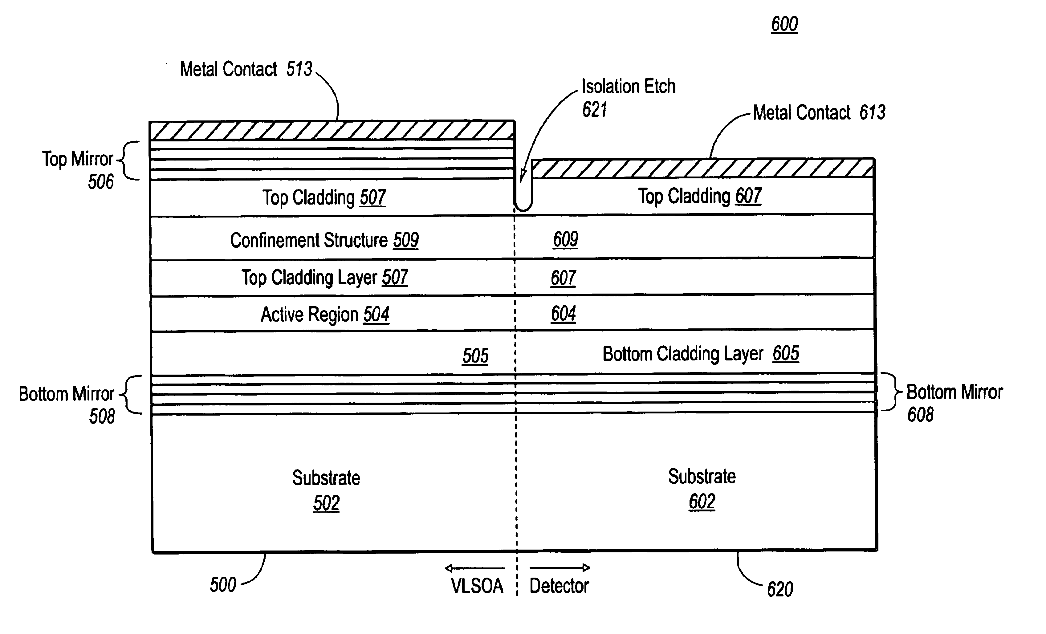
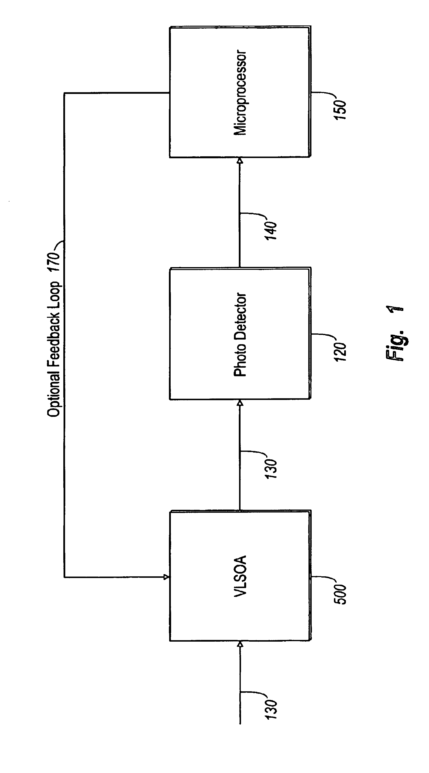
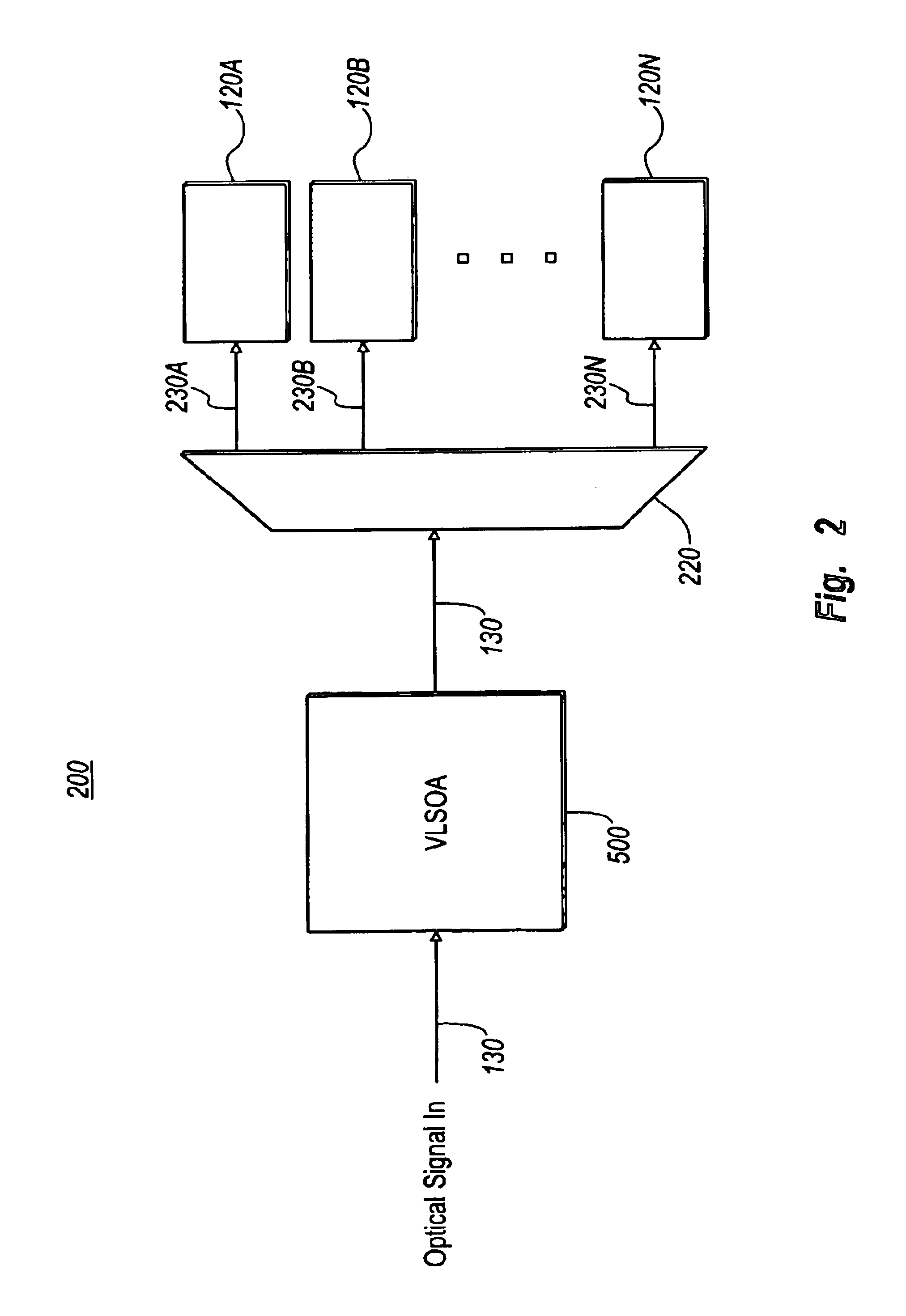
[0027]FIGS. 1 and 2 are block diagrams of example optical receivers in which a VLSOA is coupled to a photodetector, either directly or indirectly. Each of FIGS. 1 and 2 depicts a VLSOA in combination with some other optical element. In some embodiments, these combinations are implemented as combinations of discrete devices, which may be also packaged separately or which may be combined into a single package. For example, in one embodiment of FIG. 1, the VLSOA 500 and photodetector 120 are separate discrete devices, and they are coupled together by optical fibers 130. In a preferred embodiment, the combinations shown in FIGS. 1 and 2 are implemented as integrated optics, in which multiple optical elements are integrated onto a common substrate. Applying this approach to FIG. 1, the VLSOA 500 and photodetector 120 are integrated onto a common substrate to make a single chip transmitter. The integrated and discrete approaches may be combined to form hybrid versions. For example, in FIG...


PUM


Abstract

An improved optical receiver comprises a vertically lasing semiconductor optical amplifier (VLSOA) coupled to a photodetector. The VLSOA and photodetector are discrete devices or alternatively integrated onto a common substrate. The integrated optical receiver may be fabricated using a number of different methods, including based on selective area epitaxy, impurity induced disordering, etch and fill and silicon optical bench.

Description

CROSS-REFERENCE TO RELATED APPLICATIONS[0001]This application claims priority under 35 U.S.C. § 119(e) to U.S. Provisional Patent Application Ser. No. 60 / 274,419, “Optical Receiver Including a Linear Semiconductor Optical Amplifier,” by Jeffrey D. Walker and James A. Witham, filed Mar. 9, 2001; and U.S. Provisional Patent Application Serial No. 60 / 255,753, “Optical Devices including a Semiconductor Optical Amplifier,” by Jeffery D. Walker et al., filed Dec. 14, 2000.[0002]This application is a continuation-in-part of pending U.S. patent application Ser. No. 10 / 014,679, “Integrated Optical Device Including a Vertical Lasing Semiconductor Optical Amplifier,” by Jeffrey D. Walker et al., filed Dec. 11, 2001.[0003]The subject matter of all of the foregoing is incorporated herein by reference in their entirety.BACKGROUND OF THE INVENTION[0004]1. Field of the Invention[0005]This invention relates generally to semiconductor optical amplifiers. More particularly, it relates to vertically la...

Claims


Application Information

Patent Timeline
Patent Type & Authority Patents(United States)
IPC IPC(8): H04B10/06H01S3/00H01S5/026H01S5/0683H01S5/183H01S5/22H01S5/50H04B10/158
CPCH04B10/673H04B10/67H01S5/0264H01S5/0683H01S5/1032H01S5/18311H01S5/2027H01S5/22H01S5/5072H01S5/18369
Inventor WALKER, JEFFREY D.WITHAM, JAMES A.DIJAILI, SOL P.WACHSMAN, JOHN M.
Owner II VI DELAWARE INC
Why Eureka
Try Eureka