
Eureka
For R&D, Eureka makes reading and utilizing patents & technical documents easy.
Eureka AIR
Designed for self-driven R&D workflows. Generate viable solutions, solve complex R&D challenges, empower your innovation with AI.

Eureka Materials
Designed for material experts only. Revolutionize your material R&D, from search, analyze, to developing new materials.

TechResearch
Generate reliable direction feasibility study reports for your R&D in just a few steps.

TechSeek
Discover and master advanced knowledge NOW. Basics, ideas, possibilities, all at once.

TechMind
As an expert in R&D Theories, TechMind can generates customized viable solutions instantly.

TechRisk
Analyze your overall solution with one click, know your potential R&D risks in advance.

TechMonitor
Get weekly tech updates, stay abreast of the latest tech innovations and key insights.
Data read circuit in a semiconductor device featuring reduced chip area and increased data transfer rate
- Summary
- Abstract
- Description
- Claims
- Application Information
AI Technical Summary
Benefits of technology
Problems solved by technology
Method used
Image

Examples
first embodiment
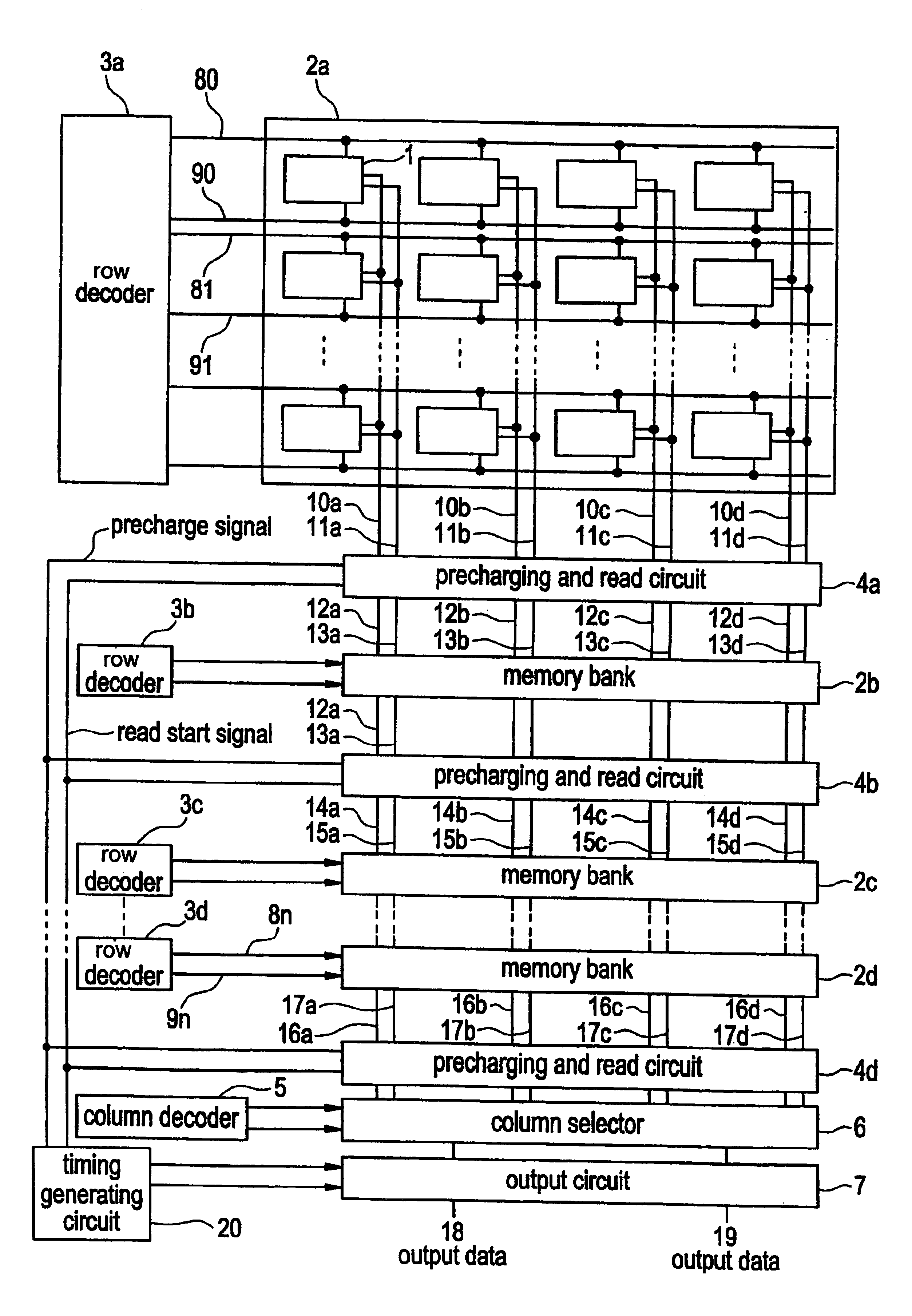
[0040]Referring now to FIG. 8, a data read circuit according to the first embodiment of the present invention comprises: memory banks 2a, 2b, 2c, and 2d that are each constructed such that a plurality of memory cells 1 are each arranged at the intersections of orthogonal horizontal lines and vertical lines; row decoders 3a, 3b, 3c, and 3d for selecting word lines; precharging and read circuits 4a, 4b, and 4d that are connected to the bit lines of a higher-order memory bank; column decoder 5; column selector 6; output circuit 7, and timing generation circuit 20 for generating precharging signals and read start signals and supplying these signals to precharging and read circuits 4a, 4b, and 4d.
[0041]Memory banks 2a, 2b, 2c, and 2d each include word lines 80, 81˜8n and 90, 91n˜9n that connect to the memory banks. Memory banks 2a, 2b, 2c, and 2d each have the same construction, and for clarity, only the construction of bank 2a will be explained, and explanation of the other banks will ...
second embodiment
[0057]FIG. 11 shows an example in which, as the second embodiment of the present invention, the above-described determination circuit is applied to the bit lines of ROM. Specifically, this embodiment comprises memory banks 20a and 20b that are constructed by arranging ROM cells at the intersections of horizontal lines and vertical lines that are arranged in intersecting form; word lines 81n8n that are connected to each of memory banks 20; precharging and read circuit 4d that is connected to bit lines 10a, 10b, 10c, and 10d of higher-order memory bank 20a; the output of this being connected to corresponding bit lines 12a, 12b, 12c, and 12d of lower-order memory bank 20b. The basic construction of this embodiment is ROM having a two-bank construction in which precharging and read circuit 4e is connected to the bit lines of lower-order memory bank 20b, and of the output of this precharging and read circuit 4e, data that have been selected by column selector 6 are supplied as output fro...
third embodiment
[0061]Referring now to FIG. 12, the third embodiment is an example in which the present invention has been applied to a logic circuit in which, as shown in FIG. 13, a wired OR circuit is connected to signal line 57 that has been precharged by PMOS transistor 31, which is a precharging transistor.
[0062]One example of this type of wired OR circuit is a Match Line in a CAM (Content Addressable Memory) having a search capability. A Match Line is a signal line for communicating the data search results of the CAM, this Match Line changing to low level if there is even one non-matching data.
[0063]In FIG. 13, if one or more of the input signals 23˜28 of logic circuits 105˜110 that are connected by wired OR to precharged signal line 57 is high level, precharged signal line 57 is discharged, thereby changing the signal level of signal line 57 to low level and changing the output signal of inverter 33 to high level.
[0064]When a large number of wired OR logic circuits are connected in a circuit...
PUM
 Abstract
Description
Claims
Application Information
 - R&D Engineer
- R&D Manager
- IP Professional
- Industry Leading Data Capabilities
- Powerful AI technology
- Patent DNA Extraction
Browse by: Latest US Patents, China's latest patents, Technical Efficacy Thesaurus, Application Domain, Technology Topic, Popular Technical Reports.
© 2024 PatSnap. All rights reserved.Legal|Privacy policy|Modern Slavery Act Transparency Statement|Sitemap|About US| Contact US: help@patsnap.com