Method of forming semiconductor device containing oxide/nitride/oxide dielectric layer

a dielectric layer and semiconductor technology, applied in the field of semiconductor devices, can solve the problems of difficult control of the thickness of the first oxide layer within a small value, difficult to form a thin thermal oxide layer over the floating gate composed of doped polysilicon, and difficult to form a thin thermal oxide layer over the floating gate, etc., to achieve high reliability, improve capacitance, and improve the effect of reliability

Inactive Publication Date: 2005-07-05
SAMSUNG ELECTRONICS CO LTD
View PDF5 Cites 34 Cited by
  • Summary
  • Abstract
  • Description
  • Claims
  • Application Information

AI Technical Summary

Benefits of technology

[0012]Thus, there exists a need to provide a semiconductor device with an oxide / nitride / oxide (ONO) dielectric layer of high reliability. There also exists a need to provide a method of fabricating a semiconductor device having an ONO dielectric layer which has an improved capacitance with high reliability. In addition, there exists a need to provide a method of fabricating a nonvolatile memory device having a large coupling coefficient.
[0013]The present invention satisfies these needs by providing a semiconductor device having an ONO layer of high reliability. The invention also provides a method of making a semiconductor device having an ONO dielectric layer with improved capacitance with high reliability, as well as a method of making a non-volatile memory device having a large coupling coefficient.

Problems solved by technology

The electrically erasable and programmable ROM (EEPROM) and flash memory are types of nonvolatile memories that are rewritable, except that rewriting is far more time-consuming than just reading.
It is very difficult, however, to form a thin thermal oxide layer over the floating gate composed of doped polysilicon.
In addition, as the doping concentration of the polysilicon is increased, the thickness of the thermal oxide layer formed on the polysilicon is increased by oxidation enhancement, so that it is very difficult to control the thickness of the first oxide layer within a small value and make the layer thinner.
Further, if the first oxide layer of the dielectric interlayer is formed over the floating gate by thermal oxidation, the reaction between oxygen and silicon is inadequately made in the corners of the floating gate that have less silicon lattices.
Hence, the thickness of the first oxide layer becomes much thinner in the corners than in the side and upper parts, so that the electric field is concentrated in the corners which degrades the breakdown characteristics.

Method used


Image

  • Method of forming semiconductor device containing oxide/nitride/oxide dielectric layer
  • Method of forming semiconductor device containing oxide/nitride/oxide dielectric layer
  • Method of forming semiconductor device containing oxide/nitride/oxide dielectric layer

Examples


examples

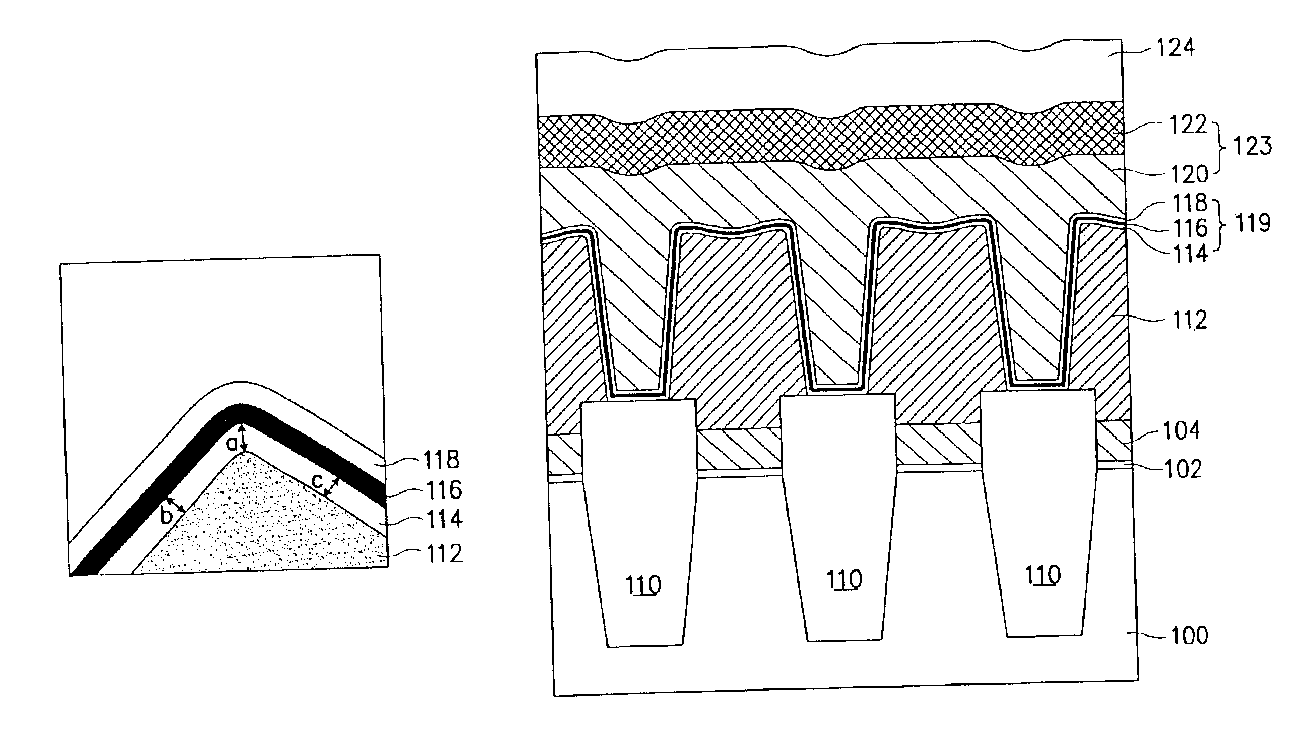
[0064]The following description reveals the results of experiments carried out in an effort to compare the charge retention property of the inventive LPCVD ONO dielectric interlayer 119 with those of the conventional ONO dielectric interlayer obtained by thermal oxidation. In these experiments, the target thickness of the ONO dielectric interlayer was determined to be 160 Å. The thickness of the conventional ONO dielectric layer was measured to be about 190 Å, and that of the inventive LPCVD ONO was about 160 Å, as determined by TEM (Transmission Electron Microscopy). The reason for the difference in thickness of the respective ONO dielectric layers was believed to be caused by the low oxide layer of the conventional ONO dielectric layer being grown to a thickness of about 40 Å over the bare wafer, while the upper oxide layer was grown to a thickness of about 84 Å over the floating gate polysilicon layer due to the oxidation enhancement caused by the dopants. In addition, the thickn...


PUM


Abstract

A semiconductor device and a method of forming the semiconductor device are disclosed. The semiconductor device includes: a semiconductor substrate; a patterned floating gate formed on the semiconductor substrate, the patterned floating gate having upper and side parts and corners; and a dielectric layer containing a first oxide layer, a nitride layer and a second oxide layer deposited over the semiconductor substrate and the floating gate. The ratio of the thickness of the first oxide layer in the upper and side parts of the patterned floating gate to the thickness of the first oxide layer in the corners of the patterned floating gate does not exceed 1.4. The semiconductor device has an improved coupling coefficient, and reduced leakage current.

Description

[0001]This application is a division of application Ser. No. 09 / 465,928, filed Dec. 17, 1999, now abandoned.BACKGROUND OF THE INVENTION[0002]1. Field of the Invention[0003]The present invention relates to a semiconductor device, and more particularly, to a method of forming a semiconductor device having a dielectric layer composed of an oxide, a nitride, and an oxide layer.[0004]2. Description of Related Art[0005]Semiconductor memory devices generally are characterized as volatile memory devices, such as DRAM (dynamic random access memory) and SRAM (static random access memory), and nonvolatile memory devices, such as ROM (read only memory), according to how they lose their stored content when the power is cut off. The electrically erasable and programmable ROM (EEPROM) and flash memory are types of nonvolatile memories that are rewritable, except that rewriting is far more time-consuming than just reading. Thus, they typically are used as special-purpose memories where writing is s...

Claims


Application Information

Patent Timeline
Patent Type & Authority Patents(United States)
IPC IPC(8): H01L27/115H01L21/70H01L29/51H01L21/8247H01L29/40H01L21/31H01L21/318H01L21/76H01L29/788H01L29/792
CPCH01L27/115H01L27/11521H01L29/511H10B69/00H10B41/30H01L21/31
Inventor CHUNG, BYUNG-HONG
Owner SAMSUNG ELECTRONICS CO LTD
Why Eureka
Try Eureka