CMOS integrated circuit devices and substrates having buried silicon germanium layers therein and methods of forming same

a technology of integrated circuits and substrates, which is applied in the direction of light-sensitive devices, transistors, electrolytic capacitors, etc., can solve the problems of reducing affecting the performance of short-channel devices, so as to improve the pmos device characteristics, inhibit the effect of punching, and increase the drive current capability of pmos transistors

Inactive Publication Date: 2005-07-05
SAMSUNG ELECTRONICS CO LTD
View PDF38 Cites 19 Cited by
  • Summary
  • Abstract
  • Description
  • Claims
  • Application Information

AI Technical Summary

Benefits of technology

[0012]Higher drive current capability in PMOS transistors may also be achieved by reorganizing the dopant profiles in the channel region and in the body region. In particular, the different solubility of certain dopants in Si and Si1-xGex can be used advantageously to improve PMOS device characteristics. In a preferred PMOS transistor, the Si1-xGex layer is doped with an N-type dopant and the concentration of the N-type dopant in the Si1-xGex layer has a profile that decreases in the first direction towards the surface of the unstrained silicon active layer. This profile preferably has a peak level within the Si1-xGex layer and may decrease in the first direction and in a monotonic manner so that a continuously retrograded N-type dopant profile extends across the unstrained silicon active layer. This N-type dopant is preferably used to suppress punch-through in the body region, but may also be used to influence the threshold voltage of the PMOS transistor.
[0014]A further embodiment of the present invention comprises a PMOS field effect transistor having a composite semiconductor active region therein that extends on an electrically insulating layer. This composite semiconductor active region comprises a single Si1-xGex layer having a graded concentration of Ge therein that decreases monotonically in a first direction extending from a peak level within the single Si1-xGex layer towards a surface thereof. An unstrained silicon active layer is also provided that extends from a first junction with the single Si1-xGex layer to the surface. The composite semiconductor active region also has an at least substantially retrograded N-type dopant profile therein that extends to the surface and has a peak level in the single Si1-xGex layer. The total charge provided by this N-type dopant influences the threshold voltage of the PMOS transistor. The N-type dopant in the single Si1-xGex layer also significantly inhibits punch-through caused by depletion layers that may extend between the source and drain regions. Lightly doped P-type source and drain regions are also preferably provided. These regions extend in the silicon active layer and opposite the insulated gate electrode. A source-side pocket implant region of N-type conductivity is also provided and this pocket implant region extends between the lightly doped P-type source region and the single Si1-xGex layer. This pocket implant region forms rectifying and nonrectifying junctions with the source region and the single Si1-xGex layer, respectively, and operates to suppress junction leakage.
[0016]Embodiments of the present invention also include methods of forming field effect transistors by forming an insulated gate electrode on a surface of a semiconductor-on-insulator substrate. This substrate includes an electrically insulating layer, an unstrained silicon active layer on the electrically insulating layer and a Si1-xGex epitaxial layer having a graded concentration of Ge therein disposed between the electrically insulating layer and the unstrained silicon active layer. Steps are also performed to form source and drain regions of first conductivity type in the unstrained silicon active layer and also form source-side and drain-side pocket implant regions of second conductivity type that extend in the unstrained silicon active layer and in the Si1-xGex epitaxial layer. These pocket implant regions form respective P-N junctions with the source and drain regions. The step of forming an insulated gate electrode is preferably preceded by the step of implanting threshold voltage control dopants of first conductivity type into the unstrained silicon active layer. These threshold voltage control dopants may then be annealed and redistributed as a result of different dopant solubility in Si and Si1-xGex, after the insulated gate electrode has been formed, to establish a retrograded profile of threshold voltage control dopants in the Si1-xGex epitaxial layer and silicon active layer. The dopants in the Si1-xGex epitaxial layer also inhibit punch-through in PMOS devices and reduce floating body effects in NMOS devices.
[0017]The substrates and forming methods of the present invention can be utilized to form NMOS transistors having reduced floating body effects (FBE). The reduction in FBE occurs because the buried SiGe layer, having a graded Ge concentration therein, reduces the potential barrier for holes passing from the body region to the source region. Therefore, holes generated in the body region by impact ionization can more readily flow into the source region through the path of the p-Si(body) / p-SiGe(body) / n+SiGe(source) / n+Si(source). NMOS transistors having well controlled kink effect characteristics and Id v. Vg curves having evenly distributed subthreshold slope with respect to Vds can also be formed. The substrates and forming methods of the present invention can also be utilized to provide PMOS transistors having excellent drive capability resulting from higher inversion-layer carrier mobility in the channel regions. This improved drive capability is achieved by reorganizing the channel region dopants through annealing so that a retrograded dopant profile and a desired threshold voltage are simultaneously achieved. This reorganization of the channel region dopants can also be used to enhance pocket ion implantation efficiency. The threshold voltage roll-off characteristics of these NMOS and PMOS devices can also demonstrate reduced short channel effects (RSCE), and the suppressed parasitic bipolar action (PBA) in the devices can be used to reduce off-leakage current.

Problems solved by technology

Partially-depleted silicon-on-insulator (PDSOI) MOSFETs offer high speed and low power performance, but typically remain susceptible to parasitic floating body effects (FBE) which can seriously degrade device performance.
Unfortunately, although the use of strained silicon channel regions may enhance carrier mobility in both NMOS and PMOS devices, such strained regions typically degrade short channel device characteristics.

Method used


Image

  • CMOS integrated circuit devices and substrates having buried silicon germanium layers therein and methods of forming same
  • CMOS integrated circuit devices and substrates having buried silicon germanium layers therein and methods of forming same
  • CMOS integrated circuit devices and substrates having buried silicon germanium layers therein and methods of forming same

Examples


Embodiment Construction

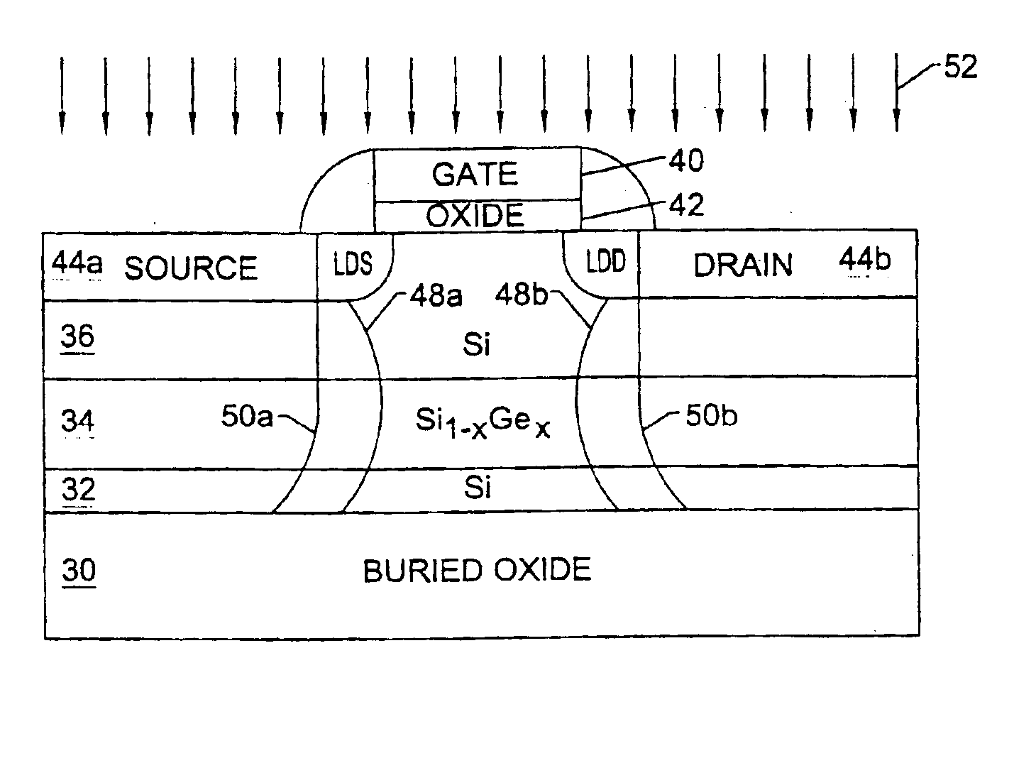
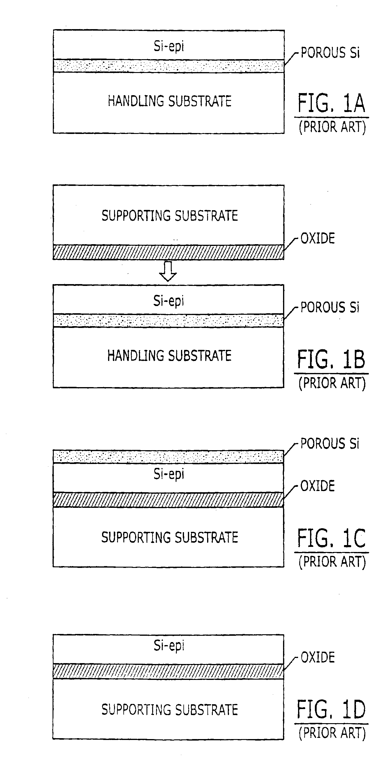
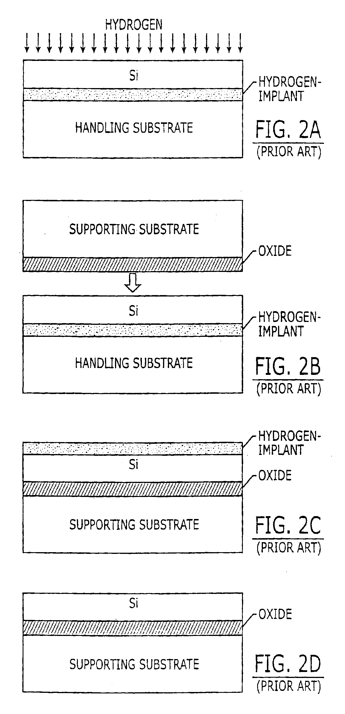
[0029]The present invention will now be described more fully hereinafter with reference to the accompanying drawings, in which preferred embodiments of the invention are shown. This invention may, however, be embodied in different forms and should not be construed as limited to the embodiments set forth herein. Rather, these embodiments are provided so that this disclosure will be thorough and complete, and will fully convey the scope of the invention to those skilled in the art. In the drawings, the thickness of layers and regions are exaggerated for clarity. It will also be understood that when a layer is referred to as being “on” another layer or substrate, it can be directly on the other layer or substrate, or intervening layers may also be present. Moreover, the terms “first conductivity type” and “second conductivity type” refer to opposite conductivity types such as N or P-type, however, each embodiment described and illustrated herein includes its complementary embodiment as...


PUM


Abstract

CMOS integrated circuit devices include an electrically insulating layer and an unstrained silicon active layer on the electrically insulating layer. An insulated gate electrode is also provided on a surface of the unstrained silicon active layer. A Si1-xGex layer is also disposed between the electrically insulating layer and the unstrained silicon active layer. The Si1-xGex layer forms a first junction with the unstrained silicon active layer and has a graded concentration of Ge therein that decreases monotonically in a first direction extending from a peak level towards the surface of the unstrained silicon active layer. The peak Ge concentration level is greater than x=0.15 and the concentration of Ge in the Si1-xGex layer varies from the peak level to a level less than about x=0.1 at the first junction. The concentration of Ge at the first junction may be abrupt. More preferably, the concentration of Ge in the Si1-xGex layer varies from the peak level where 0.2<x<0.4 to a level where x=0 at the first junction. The Si1-xGex layer also has a retrograded arsenic doping profile therein relative to the surface. This retrograded profile may result in the Si1-xGex layer having a greater concentration of first conductivity type dopants therein relative to the concentration of first conductivity type dopants in a channel region within the unstrained silicon active layer. The total amount of dopants in the channel region and underlying Si1-xGex layer can also be carefully controlled to achieve a desired threshold voltage.

Description

RELATED APPLICATION[0001]This application is a continuation of application Ser. No. 09 / 711,706, filed Nov. 13, 2000 now U.S. Pat. No. 6,633,066 which claimed priority to Korean Patent Application No. 2000-670, filed Jan. 7, 2000, the disclosures of which are hereby incorporated herein by reference.FIELD OF THE INVENTION[0002]The present invention relates to semiconductor devices and fabrication methods, and more particularly, to MOS-based semiconductor devices and substrates and methods of forming same.BACKGROUND OF THE INVENTION[0003]Partially-depleted silicon-on-insulator (PDSOI) MOSFETs offer high speed and low power performance, but typically remain susceptible to parasitic floating body effects (FBE) which can seriously degrade device performance. Various techniques have been proposed for reducing FBE in SO MOSFETs. One such technique includes using a narrow bandgap SiGe layer adjacent a source of an SOI NMOS field effect transistor. As will be understood by those skilled in th...

Claims


Application Information

Patent Timeline
Patent Type & Authority Patents(United States)
IPC IPC(8): H01L21/336H01L29/786H01L21/337H01L21/762H01L21/70H01L29/10H01L21/02H01L29/02H01L27/12H01L29/66H01L29/80
CPCH01L21/76254H01L21/76256H01L21/76259H01L21/84H01L27/1203H01L29/1054H01L29/66742H01L29/66916H01L29/78609H01L29/78612H01L29/78621H01L29/78687H01L29/802
Inventor BAE, GEUM-JONGCHOE, TAE-HEEKIM, SANG-SURHEE, HWA-SUNGLEE, NAE-INLEE, KYUNG-WOOK
Owner SAMSUNG ELECTRONICS CO LTD
Why Eureka
Try Eureka