Nitride based semiconductor light emitting device and nitride based semiconductor laser device

a technology of light-emitting devices and semiconductor laser devices, which is applied in semiconductor lasers, lasers, solid-state devices, etc., can solve the problems of difficult to reduce the threshold current in the semiconductor laser device, the growth layer is easily cracked, and the fundamental vertical transverse mode is not easily obtained, so as to achieve effective confinement of light, reduce the threshold current, and achieve the effect of reducing the yield

Inactive Publication Date: 2005-07-05
SANYO ELECTRIC CO LTD
View PDF14 Cites 6 Cited by
  • Summary
  • Abstract
  • Description
  • Claims
  • Application Information

AI Technical Summary

Benefits of technology

[0017]An object of the present invention is to provide a nitride based semiconductor light emitting device in which a threshold current can be reduced by effectively confining light in a light emitting layer without decreasing the yield due to cracking.
[0018]Another object of the present invention is to provide a nitride based semiconductor light emitting device in which an operating voltage can be reduced without decreasing the yield due to cracking.

Problems solved by technology

Accordingly, a fundamental vertical transverse mode is not easily obtained.
Therefore, it is difficult to reduce a threshold current in the semiconductor laser device.
However, the Al composition ratios are thus increased, so that a growth layer is easily cracked.
As a result, the yield of the device is greatly lowered.
Therefore, it is more difficult to reduce the threshold current in the semiconductor laser device.
Therefore, it is difficult to reduce an operating voltage in the semiconductor laser device.
Consequently, a device breakdown such as a dielectric breakdown easily occurs.

Method used


Image

  • Nitride based semiconductor light emitting device and nitride based semiconductor laser device
  • Nitride based semiconductor light emitting device and nitride based semiconductor laser device
  • Nitride based semiconductor light emitting device and nitride based semiconductor laser device

Examples


Embodiment Construction

[0065]A semiconductor laser device will be described as a semiconductor light emitting device according to the present invention.

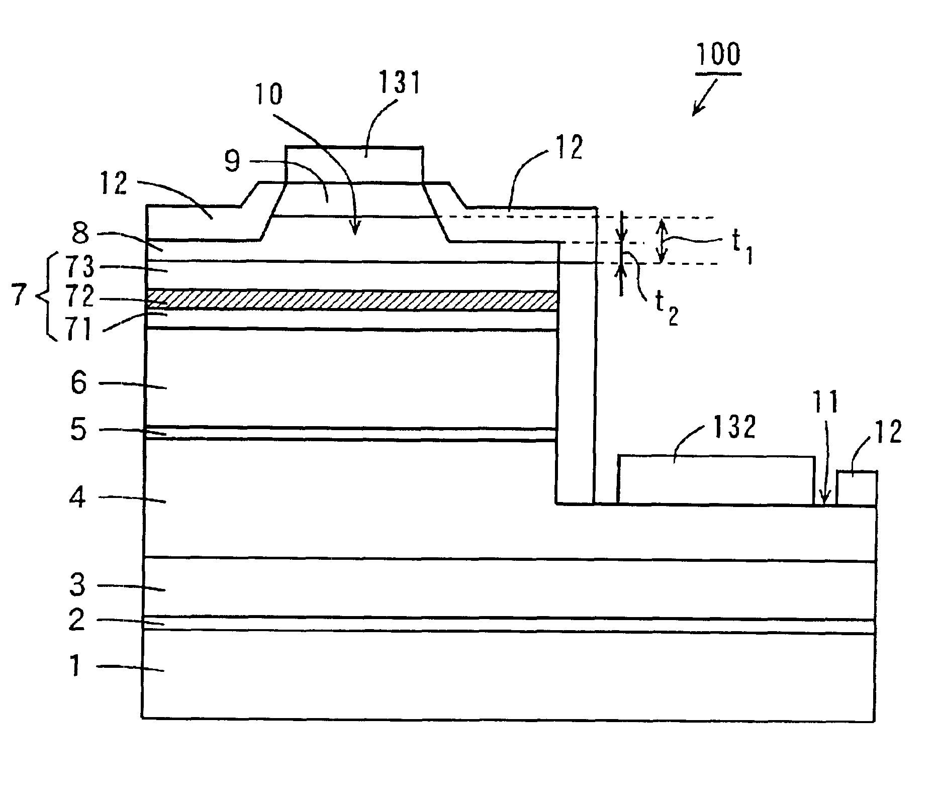
[0066]FIG. 1 is a schematic cross-sectional view showing a semiconductor laser device in an embodiment of the present invention.

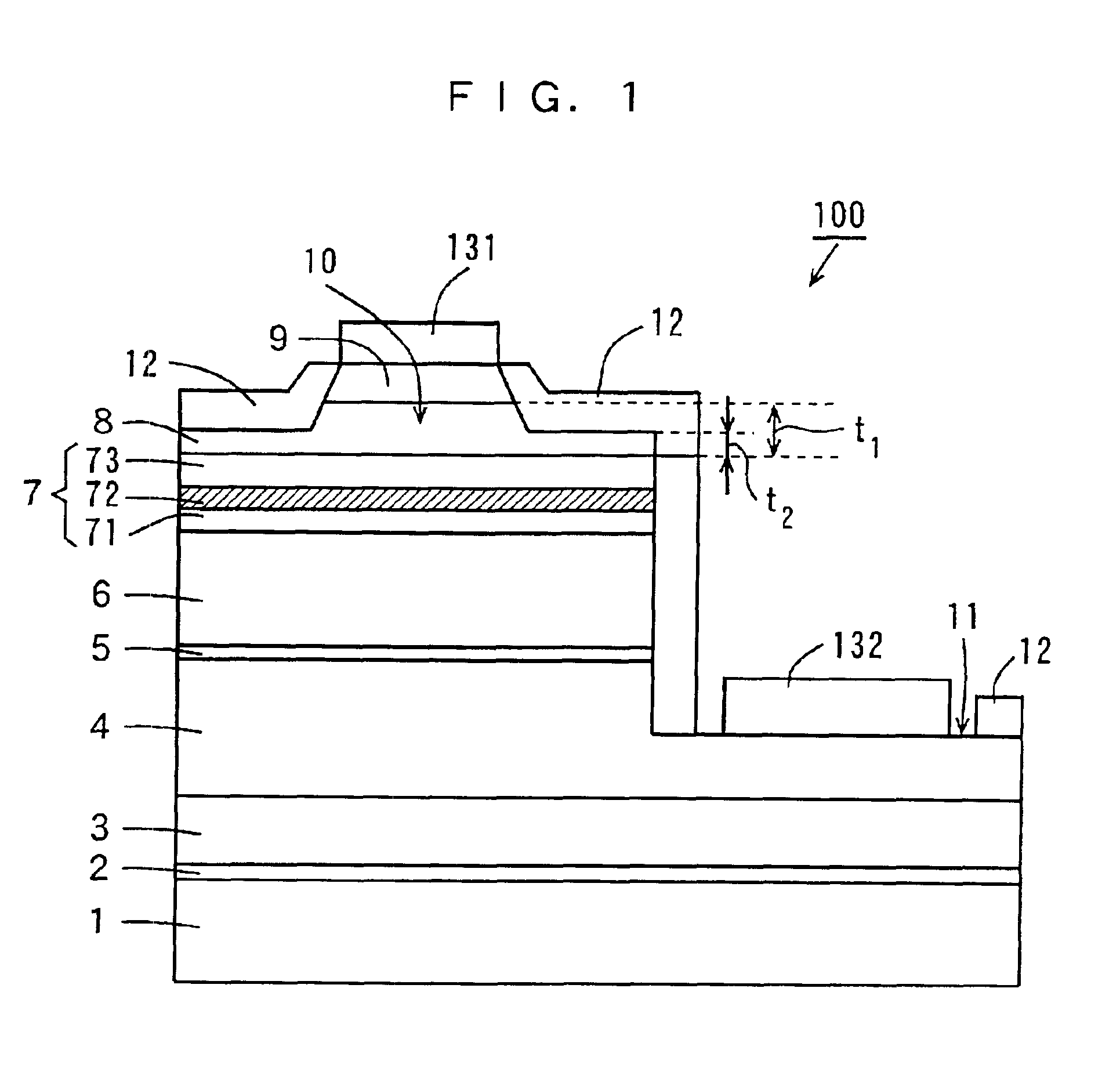
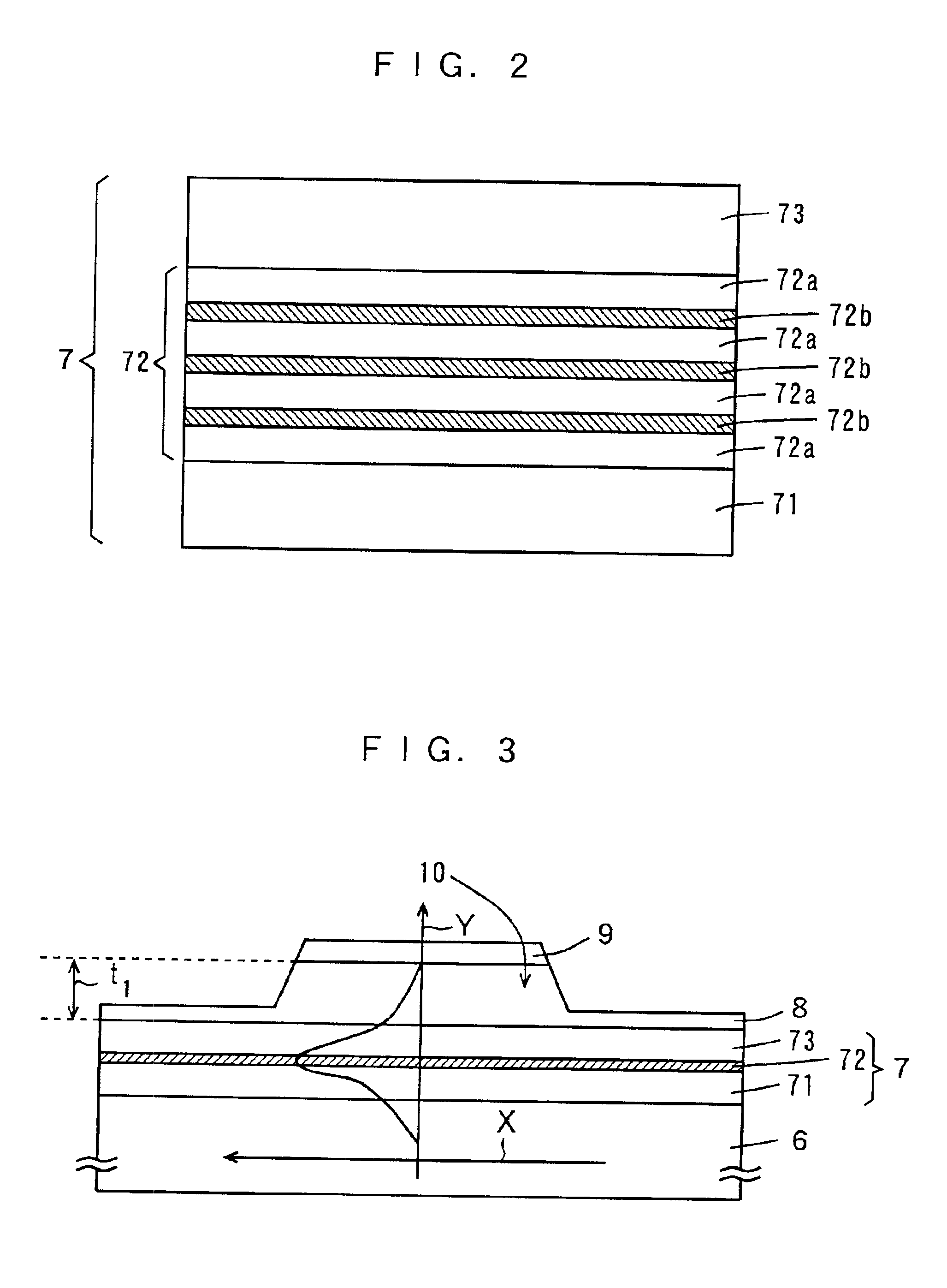
[0067]The semiconductor laser device 100 shown in FIG. 1 is constructed by forming, on the C(0001) plane of a sapphire substrate 1, a buffer layer 2 composed of undoped Al0.5Ga0.5N and having a thickness of 250 Å, an undoped GaN layer 3 having a thickness of 2 μm, an n-GaN contact layer 4 composed of Si doped GaN and having a thickness of 3 μm, an n-InGaN crack preventing layer 5 composed of Si doped In0.1Ga0.9 N and having a thickness of 0.1 μm, an n-AlGaN cladding layer 6 composed of Si doped Al0.05Ga0.95N and having a thickness of 1 μm, a light emitting layer 7, a p-AlGaN cladding layer 8 composed of Mg doped Al0.05Ga0.95N, and a p-GaN contact layer 9 composed of Mg doped GaN and having a thickness of 0.05 μm in this order. Eac...


PUM


Abstract

A semiconductor laser device is constructed by stacking a buffer layer, an undoped GaN layer, an n-GaN contact layer, an n-InGaN crack preventing layer, an n-AlGaN cladding layer, a light emitting layer, a p-AlGaN cladding layer, and a p-GaN contact layer in this order. A ridge portion comprising the p-GaN contact layer and the p-AlGaN cladding layer is formed, and the thickness of the p-AlGaN cladding layer in the ridge portion is less than 0.3 μm.

Description

BACKGROUND OF THE INVENTION[0001]1. Field of the Invention[0002]The present invention relates to a semiconductor light emitting device composed of a Group III-V nitride based semiconductor (hereinafter referred to as a nitride based semiconductor) such as BN (boron nitride), GaN (gallium nitride), AlN (aluminum nitride), InN (indium nitride) or TlN (thallium nitride) or their mixed crystal.[0003]2. Description of the Background Art[0004]In recent years, nitride based semiconductor laser devices emitting blue or violet light have been investigated and developed as light sources for recording or reproduction used for high-density and large-capacity optical disk systems.[0005]FIG. 8 is a schematic cross-sectional view showing an example of a conventional nitride based semiconductor laser device.[0006]The semiconductor laser device shown in FIG. 8 is constructed by forming, on the C(0001) plane of a sapphire substrate 81, a buffer layer 82 composed of undoped AlGaN, an undoped GaN layer...

Claims


Application Information

Patent Timeline
Patent Type & Authority Patents(United States)
IPC IPC(8): H01S5/323H01S5/00H01L33/00H01S5/20H01S5/22H01L33/14H01L33/32
CPCH01S5/32341H01L33/14H01L33/32H01S5/2004H01S5/2218H01S5/2222H01S2301/18
Inventor HAYASHI, NOBUHIKOGOTO, TAKENORIKANO, TAKASHINOMURA, YASUHIKO
Owner SANYO ELECTRIC CO LTD
Why Eureka
Try Eureka