Plastic chip-scale package having integrated passive components

Inactive Publication Date: 2005-07-12
TEXAS INSTR INC
View PDF7 Cites 6 Cited by
  • Summary
  • Abstract
  • Description
  • Claims
  • Application Information

AI Technical Summary

Benefits of technology

[0014]Another aspect of the invention is to provide a low-cost and uncomplicated process for fabrication, testing and assembly, using thin, flexible, patternable and adhesive plastic films.
[0015]Another aspect of the in

Problems solved by technology

As portable appliances continue to integrate more functionality into smaller packages, minimization of total board space becomes more critical.
On the other hand, a number of functions stubbornly resist the desired integration.
For ex

Method used


Image

  • Plastic chip-scale package having integrated passive components
  • Plastic chip-scale package having integrated passive components
  • Plastic chip-scale package having integrated passive components

Examples


Example

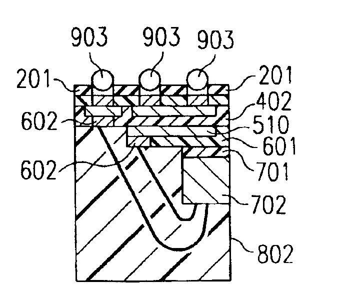
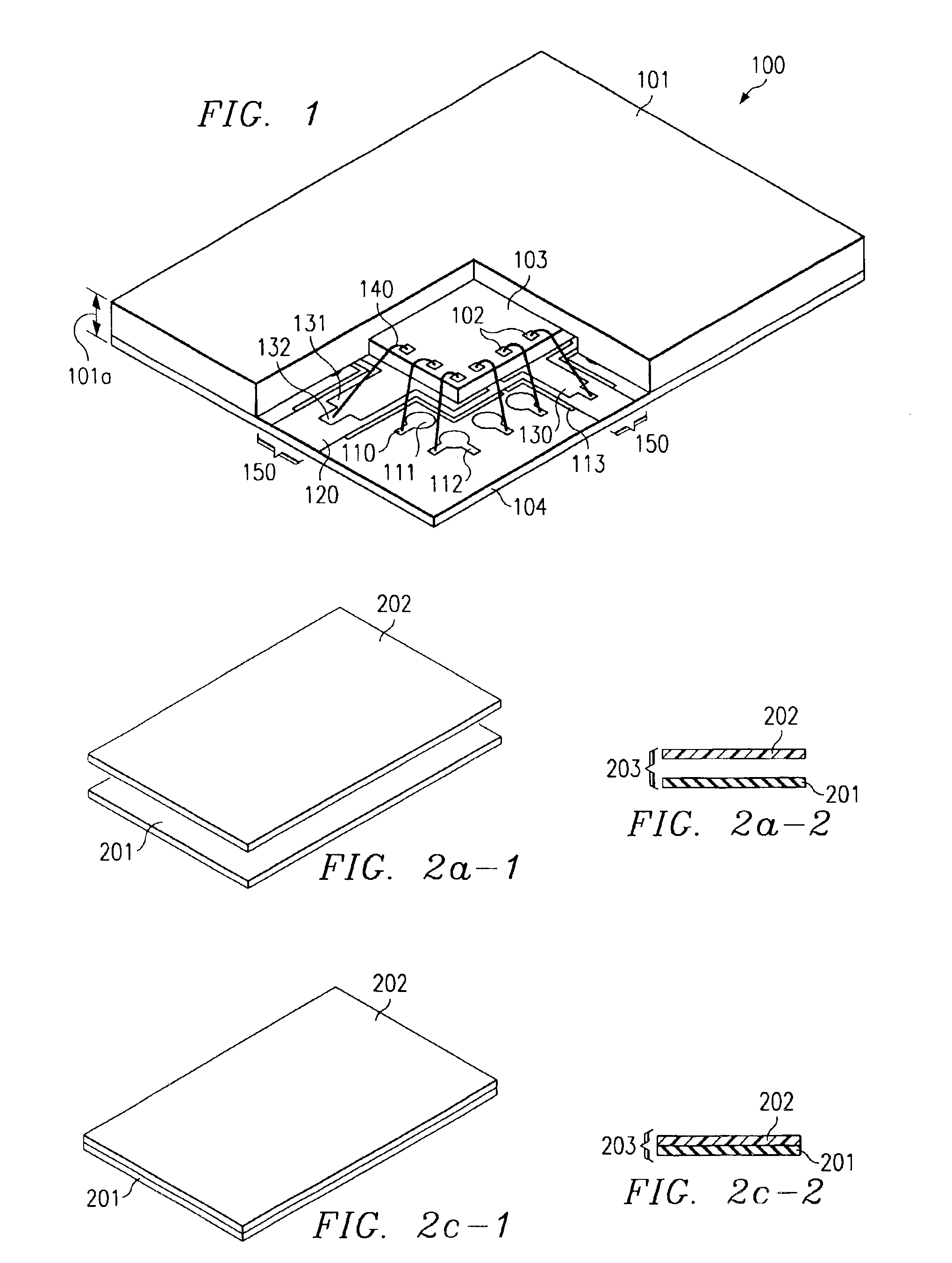
[0027]FIG. 1 illustrates a perspective, simplified view of a completed chip-scale IC device, generally designated 100, according to the invention. The device has a portion of the encapsulation 101 opened for exposing portions of the passive components 150 which are integrated with the IC chip 103 according to the invention. The illustrated device is generic; this means, additional processing can specialize it as a Land-Grid Array, Ball-Grid Array, or Pin-Grid array package.

[0028]In FIG. 1, a generic chip-scale device 100 is shown with a structure similar to the MicroStarJunior™ package fabricated by Texas Instruments, Dallas, Tex., U.S.A. In this package, a baseline polymer film 104 (for example, polyimide) is punched with an outline adding typically less than 20% to the outline of the silicon chip area. For some device types, the baseline film may have substantially the same outline.

[0029]As defined herein, the term “outline” relates to the overall width and length of the IC packag...


PUM


Abstract

A semiconductor device has passive components integrated with the circuit and encapsulated in a plastic package for solder ball or leaded attachment. A plastic chip-scale semiconductor device has a substrate made of a plurality of patterned insulating layers alternating with patterned electrically conductive layers, the layers mutually adhering to form the substrate. The layers include a plurality of passive electrical components, such as capacitors, inductors, and resistors, and routing lines. Most routing lines terminate in a first plurality of bondable contact pads and a second plurality of solderable contact pads. The components and lines form a web and are configured mostly in a narrow peripheral band at least partially around a central substrate area, and are operable with high performance in conjunction with an integrated circuit (IC) chip. The chip is attached to the central substrate area and electrically connected to the first plurality of contact pads, respectively, whereby the passive components are integrated with the IC. Plastic encapsulation material surrounds the chip, first plurality of contact pads, and passive components such that the outline of the material is approximately the same as the outline of the chip.

Description

[0001]This a divisional application of Ser. No. 09 / 855,879, filed May 15, 2001, now U.S. Pat No. 6,586,676 which is a non-provisional application claiming priority from provisional application Ser. No. 60 / 244,673, filed Oct. 31, 2000, which claims priority of provisional application Ser. No. 60 / 204,262, filed May 15, 2000.FIELD OF THE INVENTION[0002]The present invention is related in general to the field of semiconductor devices and processes, and more specifically to plastic chip-scale packages which house passive electronic components integrated with the circuit embedded in the semiconductor chip.DESCRIPTION OF THE RELATED ART[0003]As portable appliances continue to integrate more functionality into smaller packages, minimization of total board space becomes more critical. On the one hand, progress in silicon technology continues to successfully integrate more and more functionality into the silicon chip for numerous products. On the other hand, a number of functions stubbornly r...

Claims


Application Information

Patent Timeline
IPC IPC(8): H01L25/18
CPCH01L25/18H01L2224/48091H01L2224/48227H01L2224/49171H01L2224/73265H01L2924/01046H01L2924/01078H01L2924/01079H01L2924/15311H01L2924/19041H01L2924/30107H01L2924/3011H01L2924/00014H01L2924/01087H01L2224/32225H01L2924/00H01L2924/10253H01L2924/30111
Inventor PRITCHETT, SAMUEL D.COYLE, ANTHONY L.BUSCHBOM, MILTON L.
Owner TEXAS INSTR INC
Why Eureka
Try Eureka