Arrangements for reducing wavelength sensitivity in prism-coupled SOI-based optical systems

a soi-based optical system and wavelength sensitivity technology, applied in the field of arrangement for reducing wavelength sensitivity in prism-coupled soi-based optical systems, can solve the problems of inability to meet the requirements of many applications, inconvenient insertion loss, and inverse taper arrangement, so as to reduce the thickness of the evanescent coupling layer, reduce optical coupling loss, and maximize coupling efficiency

Active Publication Date: 2005-07-12
CISCO TECH INC
View PDF14 Cites 28 Cited by
  • Summary
  • Abstract
  • Description
  • Claims
  • Application Information

AI Technical Summary

Benefits of technology

[0010]In accordance with the present invention, a prism coupling arrangement is used to couple a free space optical signal into and out of a relatively thin, planar silicon waveguide (e.g., less than one micron in thickness) with an evanescent coupling layer disposed between the prism coupling arrangement and the silicon waveguide to effectuate the coupling. The refractive effects of the input / output facets of the prism coupling arrangement, as well as the characteristics of the evanescent coupling layer, are controlled and adjusted, in accordance with the present invention, to maximize the coupling efficiency between external lightwave sources of various optical signal wavelengths and the planar silicon waveguide.
[0011]In a first embodiment of the present invention, the thickness of the evanescent coupling layer is reduced (with respect to the optimum value associated with a single wavelength λc) to reduce optical coupling loss in an extended wavelength range centered around λc. In various arrangements of this first embodiment, both the material and thickness of the evanescent coupling layer may be modified to change the wavelength range of interest and / or the coupling loss over a given wavelength range. In particular, materials with a relatively large refractive index (e.g., n=2) have been found to reduce the coupling loss. Additionally, the use of a reduced-thickness evanescent coupling layer, formed of the higher refractive index material, will exhibit even less loss. Multiple materials of differing values of refractive index may be used to form a graded index evanescent coupling layer. Optical beam steering arrangements may also be employed with these modifications to the evanescent coupling layer to optimize the angle of incidence and entry point on an prism coupling input facet, further improving the coupling efficiency.
[0012]In a second embodiment of the present invention, the sensitivity to wavelength variation for a multiple-wavelength external source (such as in WDM applications) is minimized by utilizing a tapered evanescent coupling layer. The evanescent coupling layer is formed to have a monotonically increasing thickness along its input portion such that selected portions of an input beam intercept thicknesses that are under-coupled, while different selected portions of the same beam sample over-coupled thicknesses. A monotonically decreasing thickness at an output location performs the same function. Again, various materials of different refractive index may be used to form a tapered evanescent coupling layer, and / or multiple layered structures may be formed, with optical beam steering used, if desired, to further reduce wavelength sensitivity.

Problems solved by technology

While these coupling methods are relatively wavelength-insensitive, the insertion loss associated with such an arrangement increases substantially as the waveguide thickness drops below 2.0 μm.
For sub-micron thick waveguides, the dimensional mismatch between the input / output beams and the thickness of the waveguide results in an insertion loss that is unacceptable for many applications.
However, the inverse taper arrangement suffers from a number of drawbacks, such as: (1) a rapid increase in insertion loss with sub-micron misalignments; (2) the need for specialized techniques, such as e-beam lithography, to fabricate the nanotapers; and (3) the need for additional waveguiding structures prior to the tip of the nanotapers if the end of the tip is not coincident with the edge of the input facet.

Method used


Image

  • Arrangements for reducing wavelength sensitivity in prism-coupled SOI-based optical systems
  • Arrangements for reducing wavelength sensitivity in prism-coupled SOI-based optical systems
  • Arrangements for reducing wavelength sensitivity in prism-coupled SOI-based optical systems

Examples


Embodiment Construction

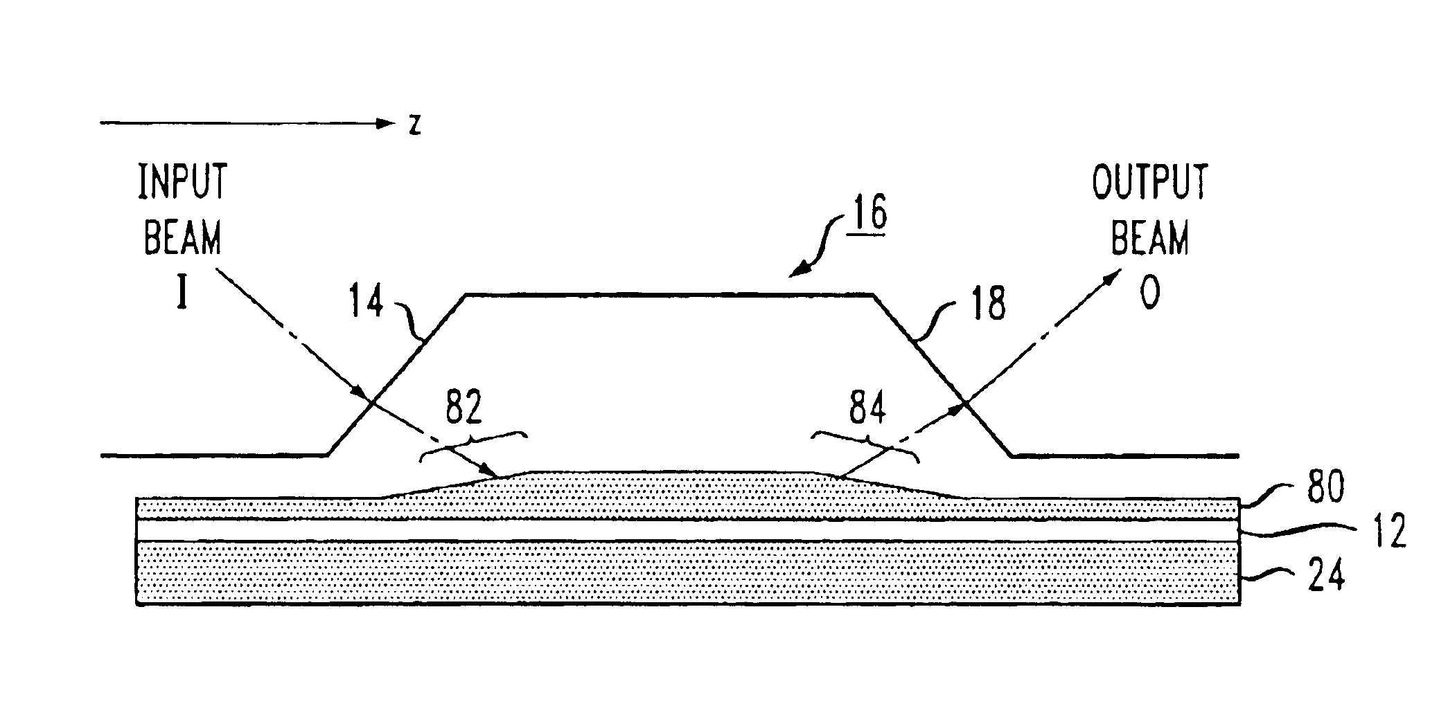
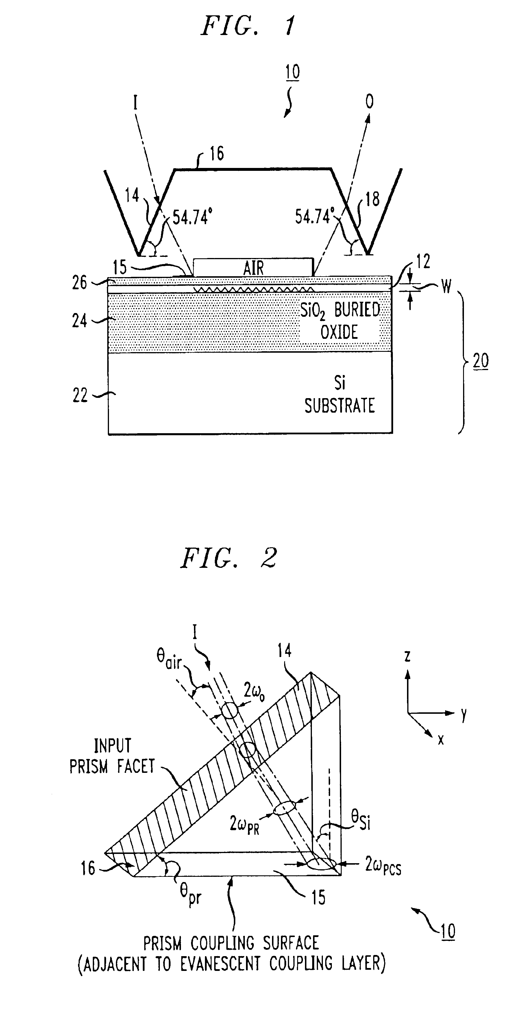
[0027]The various embodiments of the present invention are all directed to the utilization of the evanescent coupling of light into and out of thin (e.g., sub-micron) silicon waveguides that are formed within a surface single crystal silicon layer (the “SOI layer”) of an SOI structure that consists of a silicon substrate, a buried dielectric layer and the surface SOI layer. A preferred arrangement for providing optical coupling of a free space optical beam into and out of the thin silicon waveguide is to use a prism coupling arrangement, as described in detail in our co-pending applications Ser. No. 10 / 668,947, filed Sep. 23, 2003 and Ser. No. 10 / 720,372, filed Nov. 24, 2003. FIG. 1 illustrates an exemplary prism coupling arrangement 10 between free space input and output optical beams, denoted as I and O, respectively, and a thin silicon waveguide within an SOI layer 12. As shown, SOI layer 12 comprises the surface layer of an SOI structure 20 that further comprises a silicon subst...


PUM


Abstract

An optical coupling system for use with multiple wavelength optical signals provides improved coupling efficiency between a free-space optical beam and a relatively thin, surface layer of an SOI structure (“SOI layer”), allowing for sufficient coupling efficiency (greater than 50%) over a predetermined wavelength range. An evanescent coupling layer, disposed between a coupling prism and an SOI layer, is particularly configured to improve the coupling efficiency. In one embodiment, the thickness of the evanescent layer is reduced below an optimum value for a single wavelength, the reduced thickness improving coupling efficiency over a predetermined wavelength range around a defined center wavelength. Alternatively, a tapered thickness evanescent coupling layer may be used to improve coupling efficiency (or a combination of reduced thickness and tapered configuration). Optical beam steering can be combined with a modified evanescent coupling layer to control the input beam launch angle and further improve coupling efficiency.

Description

CROSS-REFERENCE TO RELATED APPLICATION[0001]This application claims the benefit of Provisional Application No. 60 / 466,307, filed Apr. 28, 2003.TECHNICAL FIELD[0002]The present invention relates to arrangements for providing optical coupling between an external source and a relatively thin silicon waveguide layer in an SOI structure and, more particularly, to arrangements for providing coupling between variable-wavelength and multiple-wavelength sources and a thin silicon waveguide layer.BACKGROUND OF THE INVENTION[0003]To meet the bandwidth requirements of current and future high speed applications, state-of-the-art telecommunication components and systems must provide a host of sophisticated signal processing and routing functions, in both the optical and electronic domains. As the complexity level increases, integration of more functions and components within a single package is required to meet system-level requirements and reduce the associated size and cost of the end system. I...

Claims


Application Information

Patent Timeline
Patent Type & Authority Patents(United States)
IPC IPC(8): G02B26/08G02B6/42G02B6/12G02B6/34
CPCG02B6/12G02B6/34G02B6/4206G02B26/0833
Inventor GHIRON, MARGARETGOTHOSKAR, PRAKASHMONTGOMERY, ROBERT KEITHPATEL, VIPULKUMARPATHAK, SOHAMSHASTRI, KALPENDUYANUSHEFSKI, KATHERINE A.
Owner CISCO TECH INC
Why Eureka
Try Eureka