Loadless NMOS four transistor dynamic dual Vt SRAM cell

a sram cell, dynamic dual-vt technology, applied in semiconductor devices, digital storage, instruments, etc., can solve the problems of limiting the density of memory cells, limiting leakage, etc., to achieve high-integration semiconductor memory devices, increase the i/o speed of data access operations, and improve performan

Active Publication Date: 2005-07-19
GLOBALFOUNDRIES U S INC
View PDF14 Cites 33 Cited by
  • Summary
  • Abstract
  • Description
  • Claims
  • Application Information

AI Technical Summary

Benefits of technology

[0012]Exemplary embodiments of the present invention include architectures for loadless, 4T SRAM cells, and methods for operating such SRAM cells, which can provide highly integrated semiconductor memory devices while providing increased performance with respect to data stability and increased I / O speed for data access operations.
[0013]In general, in one embodiment of the invention, a loadless, 4T SRAM cell comprises a pair of access transistors and a pair of pull-down transistors, all of which are implemented as N-channel transistors (NFETs or NMOSFETS), which enables such cells to be used in high density applications. In another embodiment of the invention, the N-channel access transistors have lower threshold voltages (Vt) than the N-channel pull-down transistors, which enables the SRAM cell to effectively maintain a logic “1” potential during standby. In another embodiment, the N-type pull-down transistors have larger channel widths as compared to the N-type access transistors, which enables the SRAM cell to effectively maintain a logic “0” potential at a given storage node during a read operation. In another embodiment, a method is implemented for dynamically adjusting the threshold voltages of the transistors of activated memory cells during an access operation to thereby increase the read current of the accessed memory cells.

Problems solved by technology

When the access transistors are deactivated, the storage nodes are essentially insulated from the bit lines, although some leakage can occur.
Although 6T SRAM cells can provide high speed operation and can operate with low power supply voltage, 6T cells occupy a large area, thus limiting the memory cell density.
However, a disadvantage associated with the loadless SRAM cell (10) of FIG. 1 is that the PMOS or PFET access transistors (P1) and (P2) are relatively larger as compared to NMOS or NFET devices, which can limit the cell density.
Furthermore, PFETs have slower switching speeds as compared to NFETs of the same geometry.

Method used


Image

  • Loadless NMOS four transistor dynamic dual Vt SRAM cell
  • Loadless NMOS four transistor dynamic dual Vt SRAM cell
  • Loadless NMOS four transistor dynamic dual Vt SRAM cell

Examples


Embodiment Construction

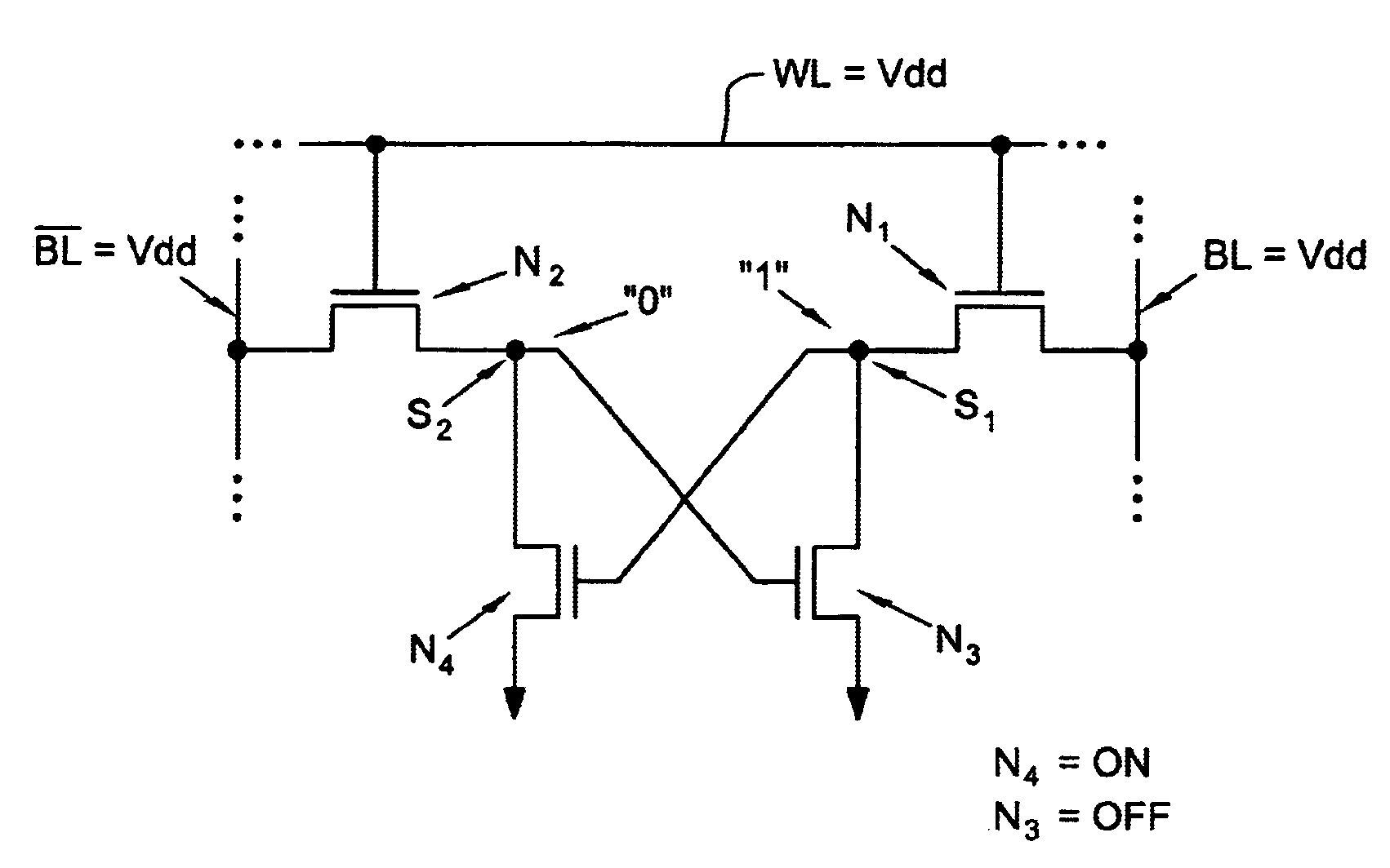
[0021]Exemplary embodiments of the present invention comprise architectures for loadless 4T SRAM cells, and methods for operating such SRAM cells, which can provide highly integrated semiconductor memory devices while providing increased performance with respect to data stability and increased I / O speed for data access operations, for example.

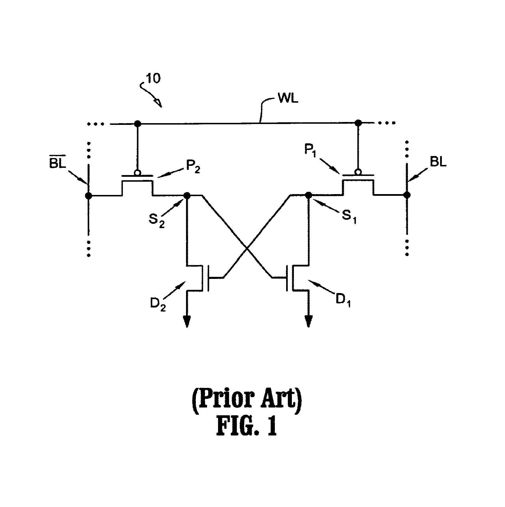
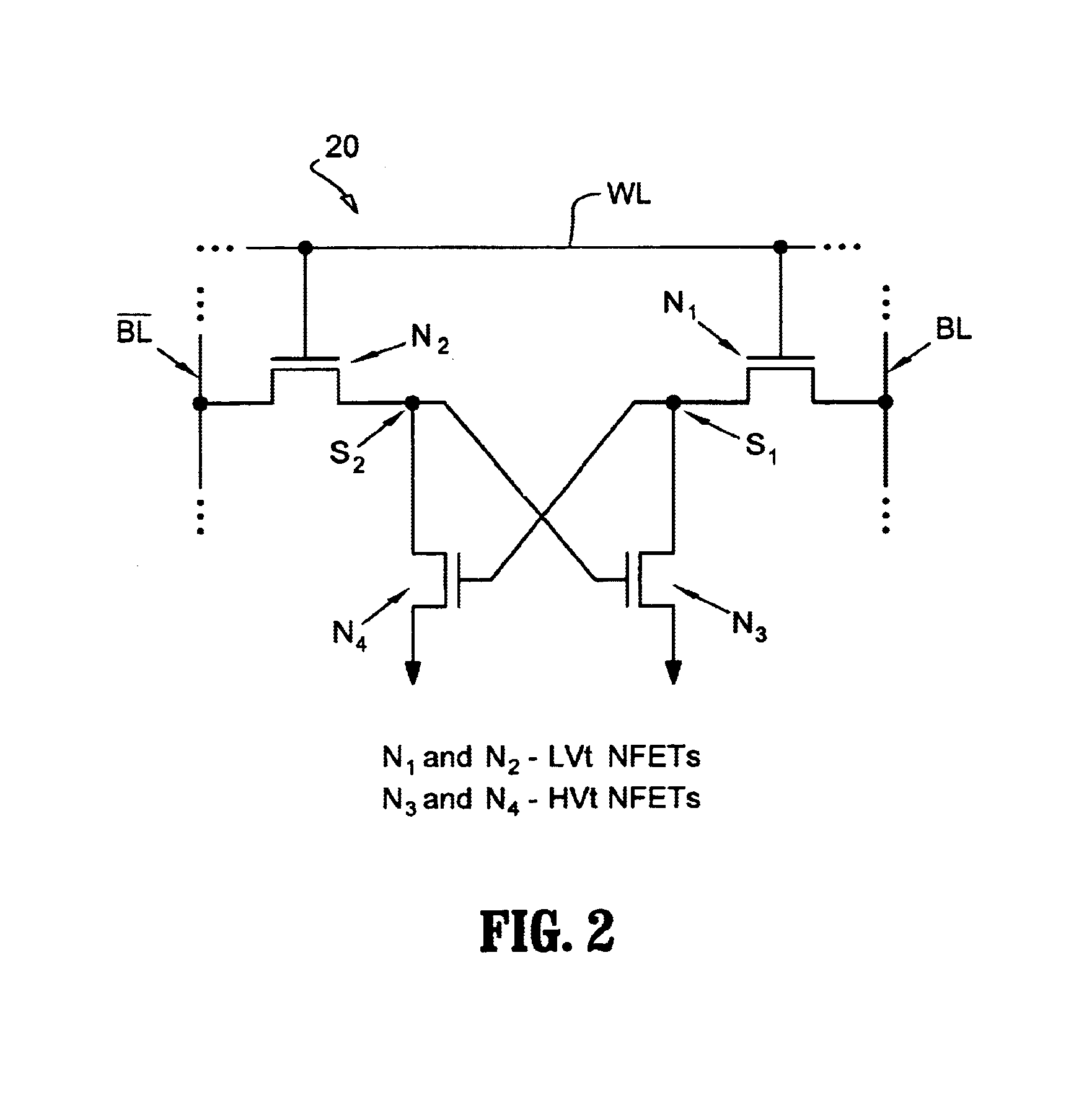
[0022]In general, in one embodiment of the invention, a loadless, 4T SRAM cell comprises a pair of access transistors and a pair of pull-down transistors, all of which are implements as n-channel transistors (NFETs or NMOSFETS). A loadless 4T SRAM cell architecture according to the present invention in which all transistors are NFETs (or NMOSFETs), for example, provides about a 50% decrease in cell area as compared to conventional 6T SRAM cells, as well as a significant decrease in the cell area as compared to conventional loadless, 4T SRAM cells that use PFETs (or PMOSFETs) as access transistors.

[0023]In another embodiment of the invention, a ...


PUM


Abstract

Loadless 4T SRAM cells, and methods for operating such SRAM cells, which can provide highly integrated semiconductor memory devices while providing increased performance with respect to data stability and increased I / O speed for data access operations. A loadless 4T SRAM cell comprises a pair of access transistors and a pair of pull-down transistors, all of which are implemented as N-channel transistors (NFETs or NMOSFETS). The access transistors have lower threshold voltages than the pull-down transistors, which enables the SRAM cell to effectively maintain a logic “1” potential during standby. The pull-down transistors have larger channel widths as compared to the access transistors, which enables the SRAM cell to effectively maintain a logic “0” potential at a given storage node during a read operation. A method is implemented for dynamically adjusting the threshold voltages of the transistors of activated memory cells during an access operation to thereby increase the read current or performance of the accessed memory cells.

Description

TECHNICAL FIELD OF THE INVENTION[0001]The present invention relates generally to semiconductor memory devices. More specifically, the invention relates to loadless, four transistor (4T) SRAM (static random access memory) cell architecture comprising four NMOSFETs (N-channel metal oxide semiconductor field effect transistors) or NFETs, and a method for accessing such SRAM cells.BACKGROUND[0002]There is a continuing demand for semiconductor memory devices with higher density and low power consumption. Semiconductor memory devices include, for example, SRAM and DRAM (dynamic random access memory) devices. Although DRAM provides a high degree of integration, SRAM is typically preferred over DRAM because SRAM cells can operate at higher speeds and lower power dissipation than DRAM cells. Indeed, SRAM cells typically do not require refreshing and can store data indefinitely as long as such cells are powered. In contrast, DRAM cells must be periodically refreshed.[0003]One well-known conve...

Claims


Application Information

Patent Timeline
Patent Type & Authority Patents(United States)
IPC IPC(8): G11C11/412G11C11/418H01L21/8244H01L27/11
CPCG11C11/412
Inventor BHAVNAGARWALA, AZEEZJOSHI, RAJIV V.KOSONOCKY, STEPHEN V.
Owner GLOBALFOUNDRIES U S INC
Why Eureka
Try Eureka