

Method of forming a liquid crystal display
a thin film transistor and liquid crystal display technology, applied in the direction of electrical equipment, semiconductor devices, instruments, etc., can solve the problems of requiring a photolithography process that tends to incur alignment errors, easy production of defects on the product, and severe problems, so as to reduce the risk and the probability of alignment errors, reduce the process, and reduce the process. effect of ion implantation process
- Summary
- Abstract
- Description
- Claims
- Application Information
AI Technical Summary
Benefits of technology
Problems solved by technology
Method used
Image

Examples
Embodiment Construction
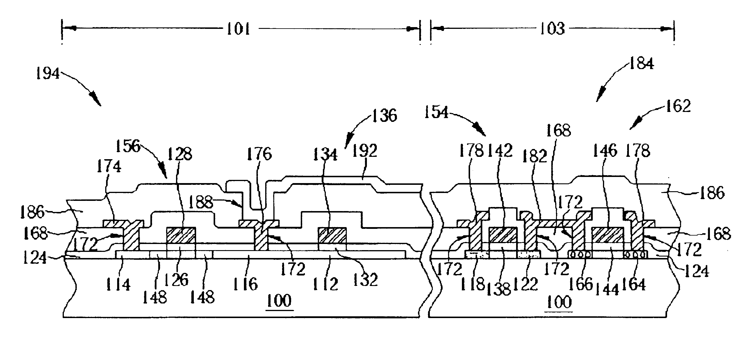
[0029]Please refer to FIG. 9 to FIG. 16 that are schematic diagrams of a method for forming a low temperature polysilicon thin film transistor liquid crystal display 194 according to a present invention. As shown in FIG. 9, the present invention low temperature polysilicon thin film transistor liquid crystal display is formed on an insulation substrate 100. The insulation substrate 100, composed of transparent materials, may be a glass substrate or a quartz substrate. A pixel array area 101 and a periphery circuit area 103 are comprised on a surface of the insulation substrate 100.
[0030]The present invention method utilizes a sputtering process or other deposition process to form an amorphous silicon thin film (α−Si thin film, not shown) on the surface of the insulation substrate 100 first. Then an excimer laser annealing (ELA) process is performed to re-crystallize the amorphous silicon thin film (not shown) into a polysilicon layer (not shown). A first photo-etching-process (PEP-...
PUM
| Property | Measurement | Unit |
|---|---|---|
| area | aaaaa | aaaaa |
| conductive | aaaaa | aaaaa |
| threshold voltage | aaaaa | aaaaa |
Abstract
Description
Claims
Application Information