Method of semiconductor device fabrication

a semiconductor device and fabrication method technology, applied in semiconductor/solid-state device manufacturing, basic electric elements, electric devices, etc., can solve the problems of increased leak current, non-uniform formation of oxide films, increased leak current, etc., and achieve high electrical reliability

Inactive Publication Date: 2005-08-09
SHARP KK
View PDF12 Cites 24 Cited by
  • Summary
  • Abstract
  • Description
  • Claims
  • Application Information

AI Technical Summary

Benefits of technology

[0007]The invention has been devised with considering these situations. An object of the invention is to provide a method of semiconductor device fabrication in which after the portions for device isolation regions are etched, a silicon fi...

Problems solved by technology

This causes the problem that leak current increases between the source region and the well region not shown so as to affect adversely the electrical c...

Method used


Image

  • Method of semiconductor device fabrication
  • Method of semiconductor device fabrication
  • Method of semiconductor device fabrication

Examples


Embodiment Construction

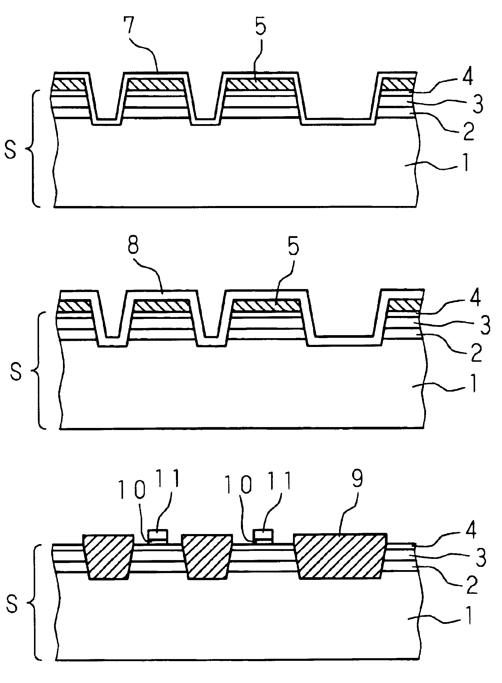
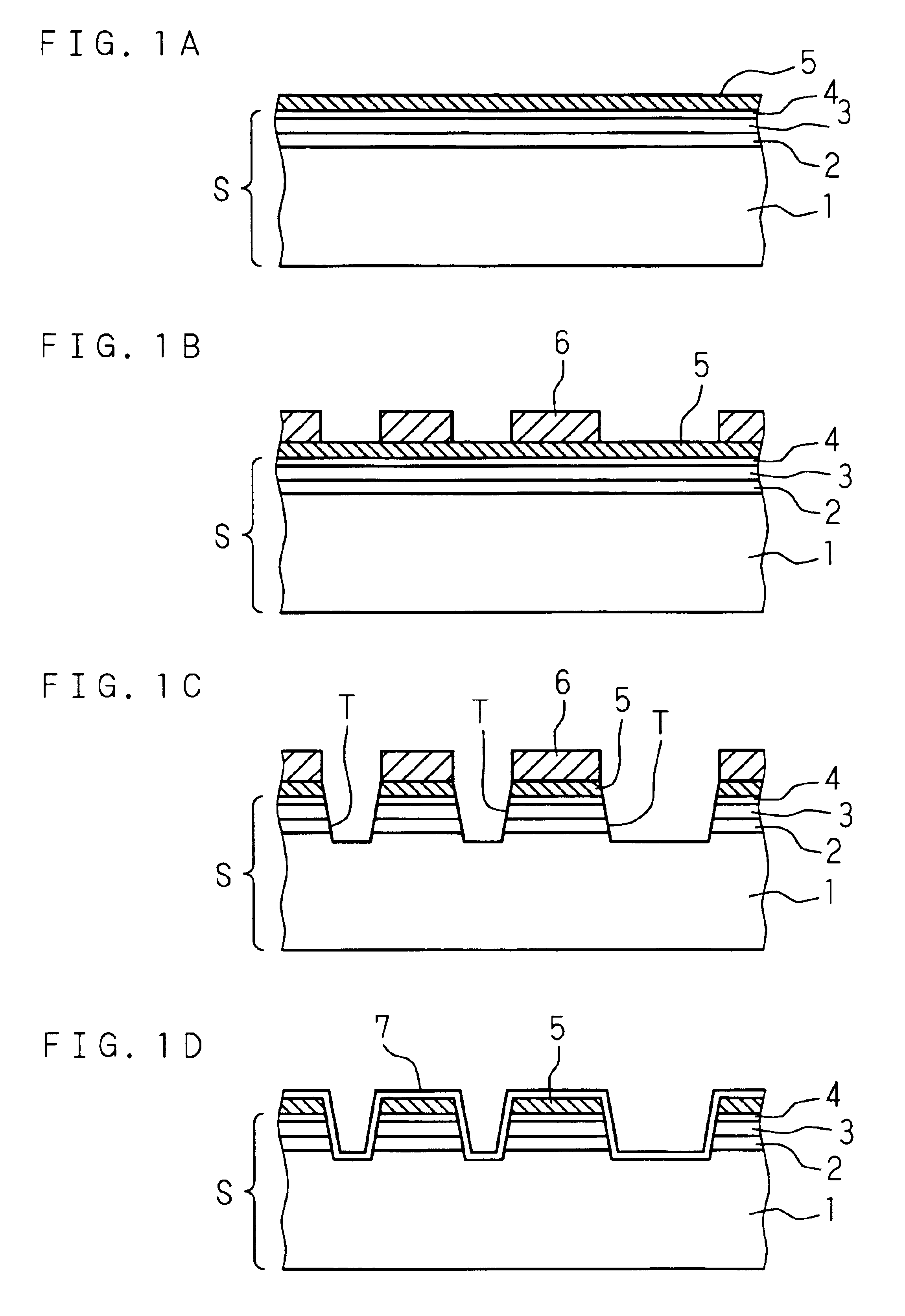
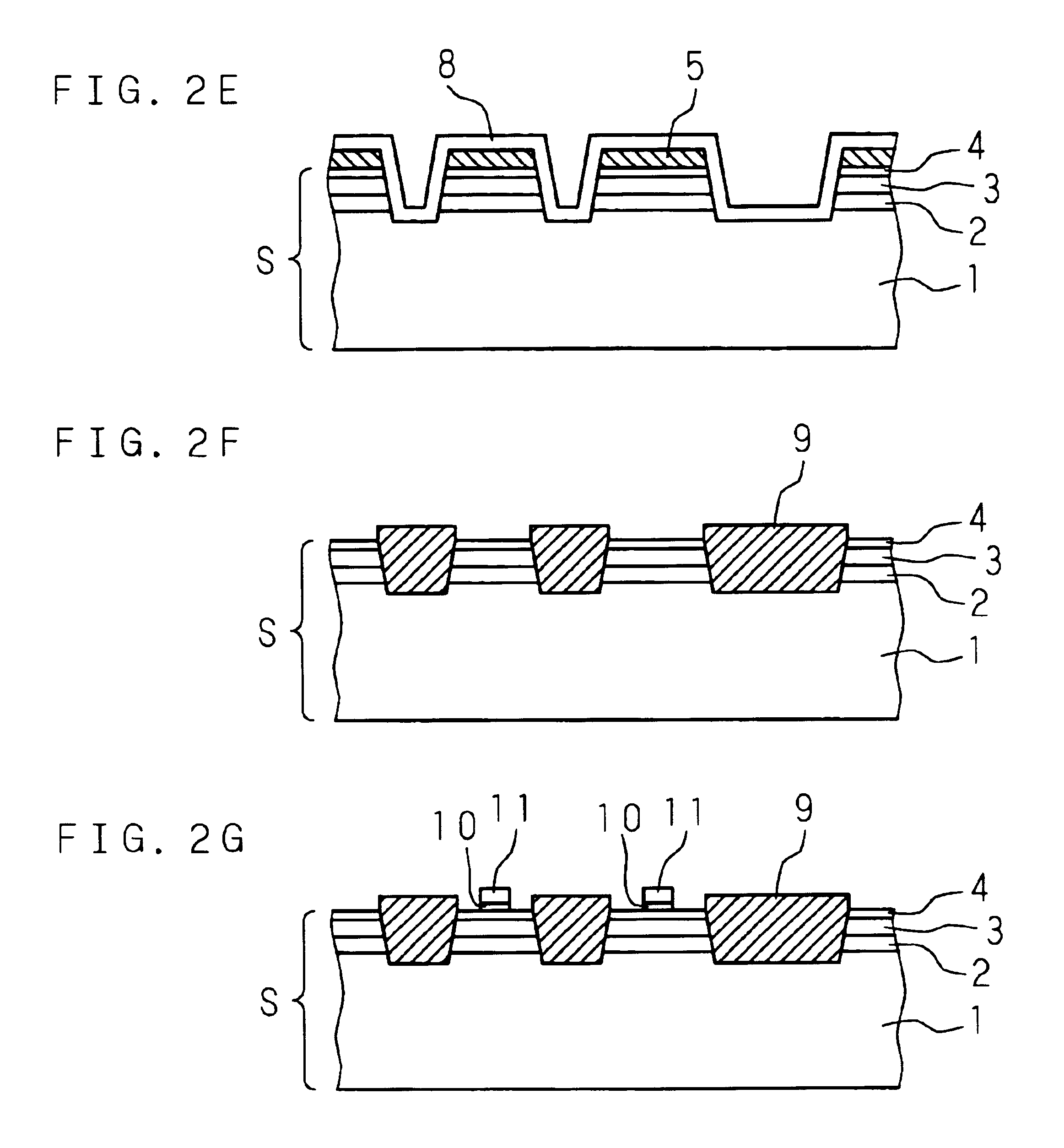
[0022]The present invention is described below with reference to the drawings illustrating the embodiments. An example of embodiment of fabricating a pair of CMOS transistors by the following processes is described below with reference to the schematic diagrams of FIGS. 1A-2G.

[0023]As a preprocess, a p-type (100) silicon substrate 1 is treated by high-temperature sulfuric acid cleaning and RCA cleaning. Then, the natural oxide film on the silicon substrate 1 is removed with 5% diluted hydrofluoric acid. Then, a silicon germanium layer 2 having a germanium concentration of 30% and a thickness of 150 nm is formed on the silicon substrate 1 by epitaxial growth at 500° C. using germanium hydride (GeH.sub.4) and silicon hydride (SiH.sub.4) in a low-pressure chemical vapor deposition (LP-CVD) system. After that, hydrogen ions are implanted into the semiconductor substrate composed of the silicon substrate 1 and the silicon germanium layer 2 under the conditions of implantation energy of 1...


PUM


Abstract

Provided is a method of semiconductor device fabrication capable of rounding the sharp edge portions of trenches so as to form device isolation regions having high electrical reliability. A semiconductor substrate comprising a lattice-strain relaxed silicon germanium layer, a silicon germanium layer, and a lattice strained silicon layer formed in this order of mention onto a silicon substrate is used, while trenches are formed in the portions for device isolation regions of the semiconductor substrate by etching. Then, a silicon film is deposited on the entirety of the exposed surface, and the deposited silicon film is dry-oxidized so as to form a silicon dioxide film. As a result, the edge portions of the trenches are rounded.

Description

BACKGROUND OF THE INVENTION[0001]The present invention relates to a method of semiconductor device fabrication using a semiconductor substrate comprising a lattice-strain relaxed silicon germanium layer formed on a silicon substrate or an SOI (silicon-on-insulator) substrate, wherein a lattice strained silicon layer is formed on said silicon germanium layer, or alternatively wherein a lattice strained silicon layer is formed on one or more semiconductor layers formed on said silicon germanium layer.DESCRIPTION OF THE RELATED ART[0002]In the prior art, a semiconductor substrate is known that is fabricated for improving the mobility of carriers (electrons or holes) passing through a channel. That is, a silicon germanium layer 22 having lattice strain is formed into a virtual lattice shape on a silicon substrate 21, while the strain in the silicon germanium layer 22 due to lattice constant incommensurate to the silicon substrate 21 is relaxed by introducing misfit dislocations. Then, a...

Claims


Application Information

Patent Timeline
IPC IPC(8): H01L21/70H01L21/762H01L21/76
CPCH01L21/76229H01L21/76235
Inventor TAKENAKA, MASAHIRO
Owner SHARP KK
Why Eureka
Try Eureka