Ion implantation method and method for manufacturing SOI wafer

a technology of ion implantation and manufacturing method, which is applied in the direction of ion beam tubes, vacuum evaporation coatings, coatings, etc., can solve the problems of low efficiency of hydrogen ions, complicated and difficult maintenance, and inability to implantation hydrogen ions at the same time, so as to achieve efficient and secure manufacturing of soi wafers and excellent integration

Active Publication Date: 2005-08-09
APPLIED MATERIALS INC
View PDF36 Cites 70 Cited by
  • Summary
  • Abstract
  • Description
  • Claims
  • Application Information

AI Technical Summary

Benefits of technology

[0012]According to the present invention, when the hydrogen gas is introduced into the vacuum chamber where the inner pressure is reduced and the predetermined magnetic field is formed, the plasma is generated by introducing the microwave into the magnetic field. Thus, generation efficiency of the hydrogen molecule ions can be enhanced by use of low-energy electrons in the plasma generation. Moreover, because an extremely high plasma density is achieved, a ratio of the hydrogen molecule ions and a current density in the hydrogen ion beams extracted from the plasma can be improved. Furthermore, the hydrogen ions can be implanted efficiently to the predetermined depth of the semiconductor substrate by irradiating the hydrogen molecule ions in the hydrogen ion beams onto the semiconductor substrate. Thus, a high level throughput becomes realizable in the manufacturing process of the SOI wafer.
[0014]Thus, the generation efficiency of the hydrogen molecule ions by the low-energy electrons is further enhanced, and the current density of the hydrogen ion beams and the ratio of the hydrogen molecule ions can be further improved.
[0015]In addition, in the ion implantation method of the present invention, it is preferable that a mean residential time of the hydrogen molecules from the introduction of the hydrogen gas into a generation region of the plasma to the extraction of the hydrogen ion beams ranges from 5×10⁻⁴ to 5×10⁻³ seconds. Thus, the generation efficiency of the hydrogen molecule ions by the low-energy electrons can be further enhanced, and the current density of the hydrogen ion beams and the ratio of the hydrogen molecule ions can be further improved.
[0020]In the foregoing first manufacturing method, the hydrogen ion implanted layer is formed to the predetermined depth of the first wafer (insulating layer / Si substrate), the second wafer is layered on the insulating layer to form the layered body (Si substrate / insulating layer / Si layer / hydrogen ion implanted layer / Si substrate), and this layered body is partitioned at the hydrogen ion implanted layer. Thus, the SOI wafer (Si layer / insulating layer / Si substrate) is obtained. In this case, by applying the ion implantation method of the present invention in the ion implantation step, the hydrogen ions are implanted efficiently to the predetermined depth of the Si substrate, thus making it possible to dramatically improve the throughput. In addition, by performing the ion implantation in this way, the formation of the hydrogen ion implanted layer to a relatively shallow position in the Si substrate from the surface of the insulating layer side can also be achieved easily. Hence, the foregoing manufacturing method is extremely useful in that it is possible to manufacture the SOI wafer efficiently and securely which is excellent in integration.
[0022]In the foregoing second manufacturing method, after the hydrogen ion implanted layer is formed on the third wafer formed of the Si substrate, an insulating layer and a fourth wafer are layered on a predetermined surface of the third wafer, and the layered body is partitioned at the hydrogen ion implanted layer. Thus, an SOI wafer (Si layer / insulating layer / Si substrate) is obtained. In this case also, by applying the ion implantation method of the present invention in the ion implantation step, it is possible to manufacture the SOI wafer efficiently and securely which is excellent in integration in a similar way to that of the first manufacturing method.
[0023]In each of the first and second manufacturing methods, it is preferable that the insulating layer is a SiO2 layer. Thus, an SOI wafer having a layered structure of Si layer / SiO2 layer / Si substrate is obtained efficiently.

Problems solved by technology

However, there are physical limitations on a plasma density in the arc discharge type ion source, and therefore, there is an upper limit on a current density of ion beams of hydrogen atoms extracted as single atom ions, causing constraints on the implantation rate of the hydrogen ions.
Therefore, efficiency thereof is low, and maintenance thereof is also complicated and difficult.

Method used


Image

  • Ion implantation method and method for manufacturing SOI wafer
  • Ion implantation method and method for manufacturing SOI wafer
  • Ion implantation method and method for manufacturing SOI wafer

Examples


Embodiment Construction

[0028]A preferred embodiment of the present invention will be described below in detail with reference to the drawings. Note that, in the drawings, the same reference numerals will be added to the same or equivalent portions, and repeated descriptions will be omitted.

[0029]First, an ion implantation method will be described.

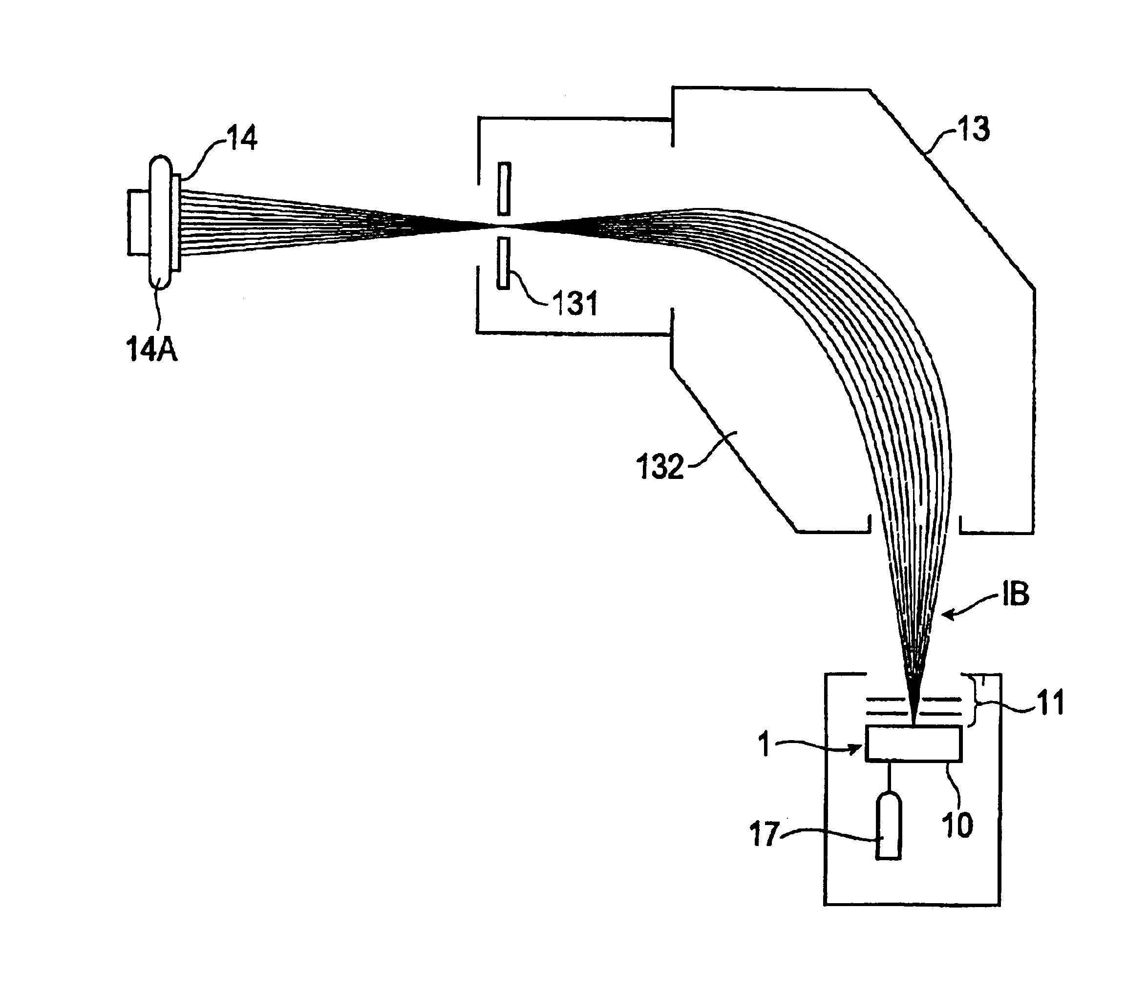
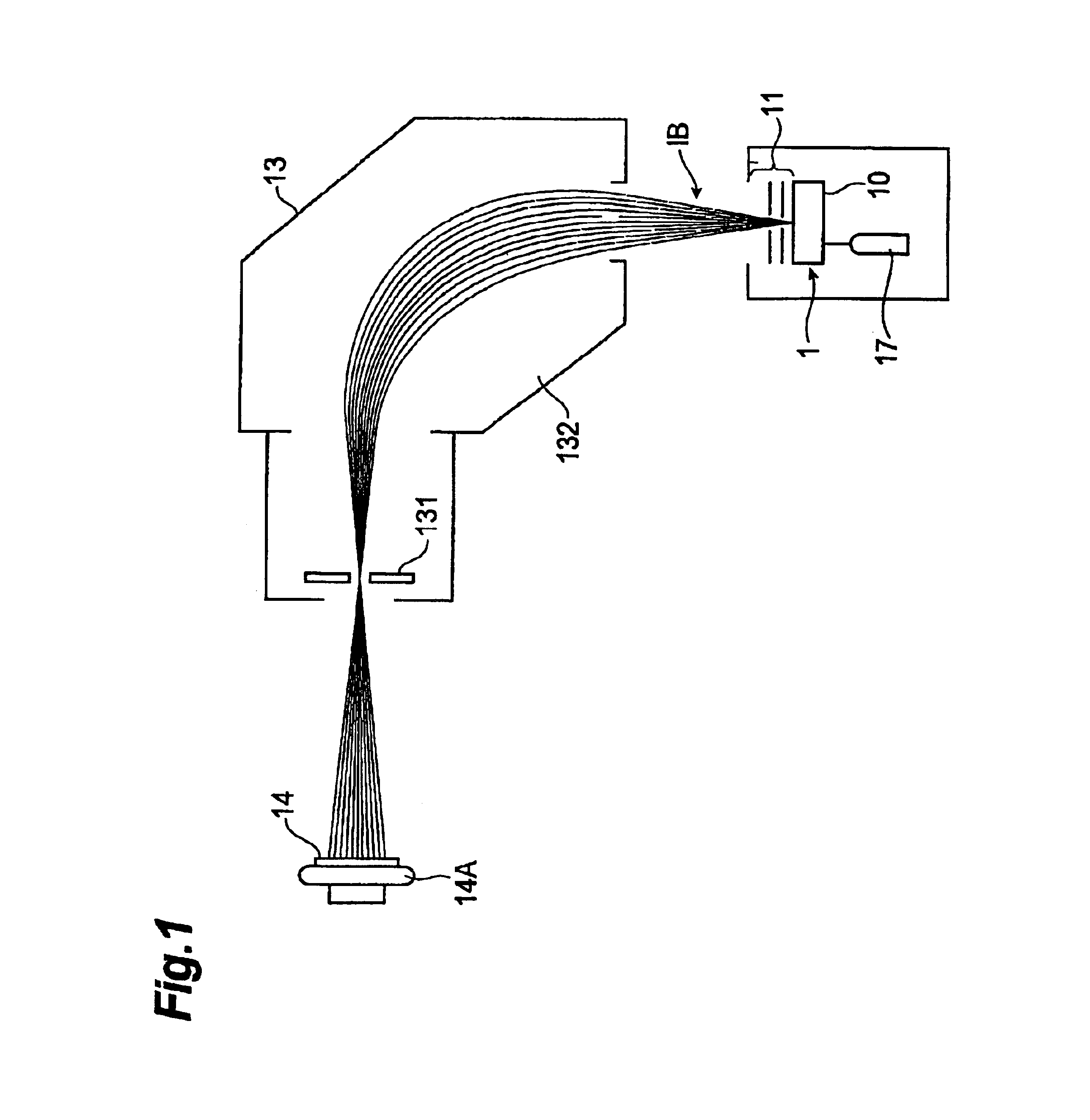
[0030]FIG. 1 is an explanatory view schematically showing an example of an ion implantation apparatus for use in the present invention. The apparatus shown in FIG. 1 is one provided with the ion extraction assembly 1 including the ion source 10, the tank 17 for supplying hydrogen gas to the ion source 10 and the extraction electrodes 11, with the ion mass selector 13, and with the target substrate folder 14A. The hydrogen ion beams IB from the ion extraction assembly 1 are directed toward the target substrate folder 14A through the ion mass selector 13. In this case, hydrogen molecule ions are selected from the hydrogen ion beams IB passing through the ion mass s...


PUM

PropertyMeasurementUnit
magnetic fieldaaaaaaaaaa

Abstract

Disclosed are an ion implantation method capable of dramatically increasing an implantation rate of hydrogen ions into a semiconductor substrate and a method for manufacturing an SOI wafer, in which manufacturing efficiency of the SOI wafer is sufficiently high. When the hydrogen ions are implanted to a predetermined depth of the semiconductor substrate, hydrogen gas is introduced into a chamber where an inner pressure is reduced and a predetermined magnetic field is formed, plasma is generated by introducing a microwave into the magnetic field, hydrogen ion beams containing hydrogen molecule ions is extracted from the plasma, and the hydrogen molecule ions are irradiated and implanted onto the semiconductor substrate. Thus, a throughput in the hydrogen ion implantation is improved, thus making it possible to enhance the manufacturing efficiency of the SOI wafer.

Description

BACKGROUND OF THE INVENTION[0001]1. Field of the Invention[0002]The present invention relates to an ion implantation method and a method for manufacturing an SOI wafer.[0003]2. Related Background of the Invention[0004]An SOI (Silicon on Insulator) wafer generally refers to a wafer formed into a layered structure of Si layer / insulating layer / Si substrate by forming a thin insulating layer and a single crystal Si layer near the surface of the Si substrate. In recent years, this SOI wafer has gained attention because the SOI wafer is excellent in that integration and operation speed thereof are higher in comparison with those of a usual bulk Si wafer.[0005]As a method for manufacturing the SOI wafer, a smart-cut method has been known (refer to Japanese Patent Laid-Open Publication 2000-12285 and so on). The smart-cut method is one for fabricating the SOI wafer in the following manner. Specifically, hydrogen ions are implanted into a Si substrate through an insulating layer (SiO2 layer ...

Claims


Application Information

Patent Timeline
Patent Type & Authority Patents(United States)
IPC IPC(8): H01L21/70H01L21/265H01L21/762H01L21/02H01J27/16C23C14/32H01J27/18H01J37/08H01J37/317H01L21/76H01L27/12
CPCH01J27/18H01J37/08H01L21/26506H01L21/76254H01J2237/31701Y10S438/961H01L21/2658
Inventor ITO, HIROYUKI
Owner APPLIED MATERIALS INC
Why Eureka
Try Eureka