High speed lateral heterojunction MISFETs realized by 2-dimensional bandgap engineering and methods thereof

a technology of lateral heterojunction and misfets, applied in the field of metal insulator semiconductor field effect transistors, can solve the problems of difficult to achieve abrupt doping profiles, traditional techniques that fail to reduce certain undesirable physical effects, and the scaling of silicon mosfets has become a major challenge, so as to achieve superb performance and scalability, optimize drive current and leakage current, and avoid tradeoffs in conventional si technology.

Inactive Publication Date: 2005-08-09
GLOBALFOUNDRIES US INC
View PDF2 Cites 46 Cited by
  • Summary
  • Abstract
  • Description
  • Claims
  • Application Information

AI Technical Summary

Benefits of technology

[0010]The objective of this invention is to provide a device structure that has superb performance and scalability. By using 2-dimensional bandgap engineering, the tradeoffs in the conventional Si technology can be avoided, and the drive current and leakage current can be optimized independently. Consequently, very high drive current and excellent turn-off characteristics can be achieved simultaneously. Moreover, the suppression of short-channel effects in such a device further allows continuous and more aggressive scaling of the MOSFET technology.

Problems solved by technology

Silicon MOSFET scaling has become a major challenge in the semiconductor industry.
Traditional techniques start to fail in reducing certain undesirable physical effects as device dimensions shrink down to the nanometer regime.
However, the abrupt doping profiles are difficult to achieve due to temperature enhanced diffusion, and these highly doped channels or pocket implant regions increase junction capacitance and band-to-band tunneling.
It has been shown by S. Thompson, et al., in “MOS scaling: transistor challenges for the 21st century,” Intel Technology Journal, Q3, 1998, that channel engineering can only decrease the circuit gate delay by ˜10% for a given technology, and it cannot provide channel length scaling for generation after generation that gate oxide and source / drain (S / D) junction depth scaling has provided.
However, two prominent problems remain in these planar devices: device scaling and control of short-channel effects.
However, SOI alone cannot remove the short-channel effects completely, and moreover, an inherent problem with SOI is the floating body effect.
However, it is a planar structure and still suffers from the short-channel effects.

Method used


Image

  • High speed lateral heterojunction MISFETs realized by 2-dimensional bandgap engineering and methods thereof
  • High speed lateral heterojunction MISFETs realized by 2-dimensional bandgap engineering and methods thereof
  • High speed lateral heterojunction MISFETs realized by 2-dimensional bandgap engineering and methods thereof

Examples


first embodiment

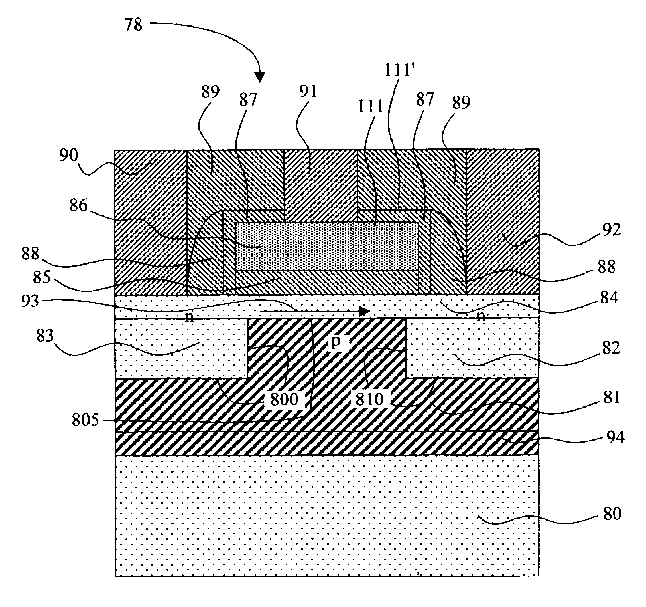
[0024]The cross sectional schematic for a SiGe based lateral nMOSFET 78 is shown in FIG. 4. The device has the following structural characteristics:[0025]1) The drain is n+-type tensile strained silicon 82;[0026]2) The body is p-type relaxed SiGe 81, and the doping level is adjusted to achieve desirable the threshold voltage;[0027]3) The source is n+-type tensile strained silicon 83;[0028]4) The channel is tensile strained Si 84, and there is no hetero-barrier along the current flow direction shown by arrow 93. The channel forms a heterojunction with the body 81 at the interface 805 which functions to provide a band offset as shown in FIG. 3 to confine electrons in the Si channel 84. The channel is typically autodoped by the layer below. Thus the channel region over the body 81 is autodped p-type, while the channel region over the source 83 and drain 82 are doped n-type. There are other ways to provide the desired doping in the channel layer and source / drain.[0029]5) A strained Si / S...

second embodiment

[0037]Besides using a relaxed SiGe as the virtual substrate to generate a tensile strained Si layer, tensile strained SiC on silicon can also be used for nMOSFET. The cross sectional schematic for such a silicon-based lateral nMOSFET 112 is shown in FIG. 5. The device has the following structural characteristics:[0038]1) The drain is n+-type tensile strained SiC 32;[0039]2) The body is p-type silicon 31, and the doping level is adjusted to achieve the desirable threshold voltage;[0040]3) The source is n+-type tensile strained SiC 33;[0041]4) The channel is silicon or tensile strained SiC 34, and there is no hetero-barrier along the current flow direction;[0042]5) A strained SiC / Si heterojunction is formed between the source and the body at the interface 820, and is preferably, aligned with the source / body metallurgical p / n junction;[0043]6) A strained SiC / Si heterojunction is formed between the drain and the body at the interface 830, and is preferably, aligned with the drain / body m...


PUM

PropertyMeasurementUnit
concentrationaaaaaaaaaa
permittivityaaaaaaaaaa
conductingaaaaaaaaaa

Abstract

A method for forming and the structure of a strained lateral channel of a field effect transistor, a field effect transistor and CMOS circuitry is described incorporating a drain, body and source region on a single crystal semiconductor substrate wherein a hetero-junction is formed between the source and body of the transistor, wherein the source region and channel are independently lattice strained with respect the body region. The invention reduces the problem of leakage current from the source region via the hetero-junction and lattice strain while independently permitting lattice strain in the channel region for increased mobility via choice of the semiconductor materials and alloy composition.

Description

RELATED APPLICATIONS[0001]This application is cross referenced to U.S. patent application Ser. No. 10 / 463,039 by Q. Ouyang and Jack O. Chu, the inventors herein, filed herewith, entitled “Low Leakage Heterojunction Vertical Transistors and High Performance Devices Thereof” which is directed to a vertical p-channel MOSFET which is incorporated herein by reference and assigned to the assignee herein.[0002]This application is further cross referenced to U.S. patent application Ser. No. 10 / 463,038 by Q. Ouyang and Jack O. Chu, the inventors herein, filed herewith, entitled “Ultra Scalable High Speed Heterojunction Vertical n-channel MISFETs and Methods Thereof” which is directed to vertical n-channel MISFETs which is incorporated herein by reference and assigned to the assignee herein.FIELD OF THE INVENTION[0003]This invention relates to semiconductor transistors and, more particularly, to a metal insulator semiconductor field effect transistor (MISFET) consisting of a conducting channe...

Claims


Application Information

Patent Timeline
Patent Type & Authority Patents(United States)
IPC IPC(8): H01L21/70H01L29/02H01L29/66H01L21/8238H01L29/80H01L29/165H01L29/78
CPCH01L21/823807H01L21/823814H01L29/802H01L29/165Y10S438/933B01D35/14
Inventor OUYANG, QIQING CHRISTINECHU, JACK OON
Owner GLOBALFOUNDRIES US INC
Why Eureka
Try Eureka