Ion implantation system and ion implantation method

a technology of ion implantation and ion implantation, which is applied in the field of ion implantation system and ion implantation method, can solve the problems of high cost and troublesome ion implantation step, and achieve the effect of small siz

Inactive Publication Date: 2005-08-16
ULVAC INC
View PDF21 Cites 61 Cited by
  • Summary
  • Abstract
  • Description
  • Claims
  • Application Information

AI Technical Summary

Benefits of technology

[0010]As above described, the small-sizing of the ion implantation system and the rationalizing of the ion implantation step have been developed. However, when ions are implanted on specified regions of a semiconductor substrate, it is required that the kinds of ions, the ion implantation energies and ion doses are changed. Plural ion implantation systems have been required.
[0011]Accordingly, it is an object of this invention to provide an ion implantation system and an ion implantation method which can be small sized and by which the kinds of ions, the ion implantation energies and the ion dose can be changed in one unit.
[0012]In accordance with an aspect of this invention, in an ion implantation system including (a) an ion source means, (b) a mass analyzing portion, (c) an ion acceleration portion, (d) an ion beam focusing/deflecting portion, and (e) an end station chamber for implanting ions onto a semiconductor substrate, the improvement resides in that the ion source means consists of plural ion sources be

Problems solved by technology

When a semiconductor substrate is large sized, such as 300 mmΦ in diameter, an ion implantation system is large-sized and causes the cost to rise.
In the conventional ion impla

Method used


Image

  • Ion implantation system and ion implantation method
  • Ion implantation system and ion implantation method
  • Ion implantation system and ion implantation method

Examples


Embodiment Construction

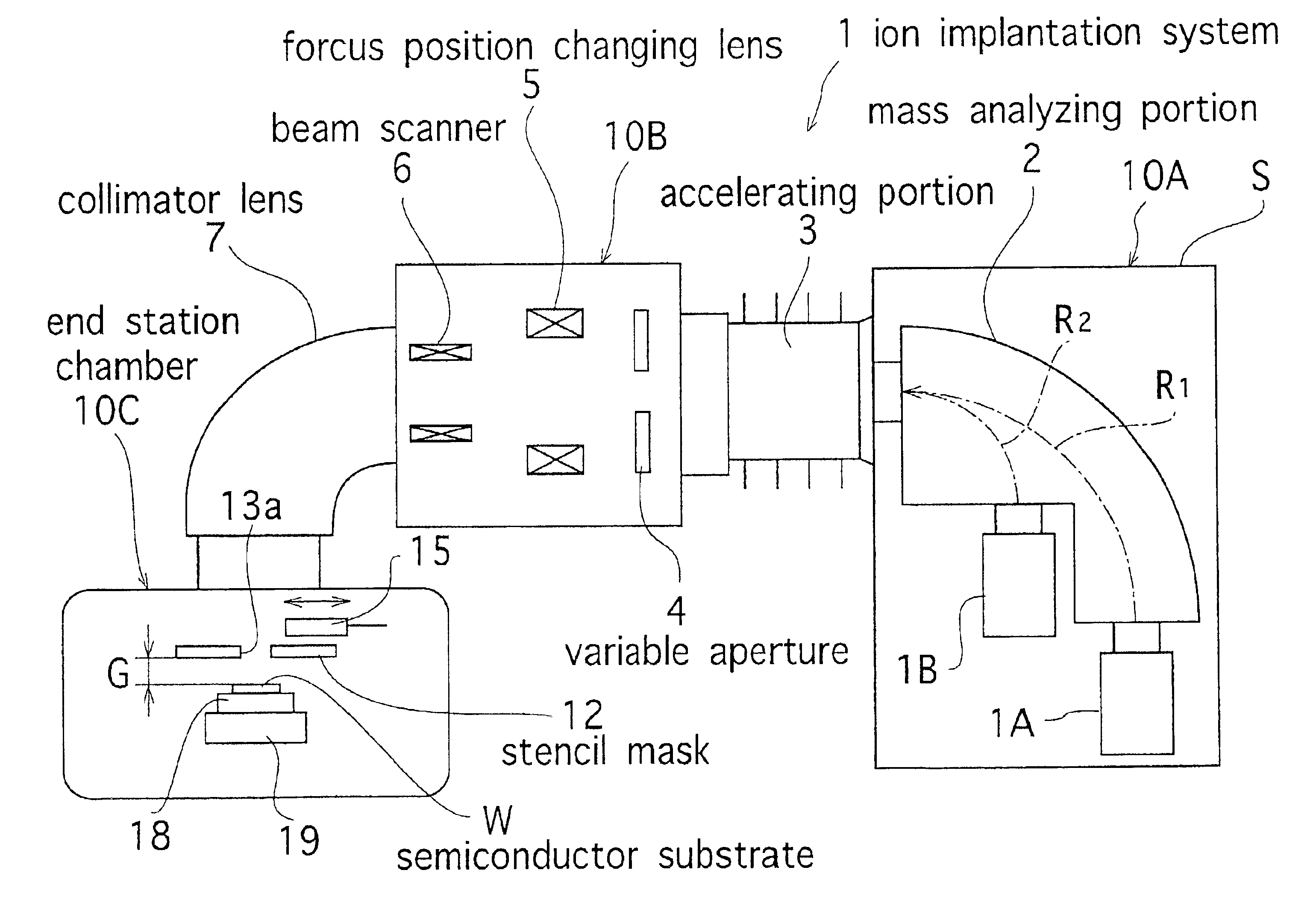
[0028]In the ion implantation system and the ion implantation method of this invention, plural ion sources, as ion source means, are connected to the same mass-analyzing portion in which the strength of applied magnetic field can be changed, and any one of the plural ion sources is selected with the strength of the applied magnetic field, and ions extracted from the selected ion source are led into the same acceleration portion.

[0029]FIG. 1 shows one example of a constitution of an ion implantation system according to this invention. An ion implantation system 1 is a vacuum system which consists of a high voltage terminal 10A, a beam line portion 10B and an end station chamber 10C. A multi-charged ion source 1A and a high current ion source 1B are arranged on the high voltage terminal 10A. The multi-charged ion source 1A is used for implanting ions at high energy, and the high current ion source 1B is used for implanting ions at high dosage. They are connected to a mass-analyzing po...


PUM

PropertyMeasurementUnit
Temperatureaaaaaaaaaa
Massaaaaaaaaaa
Diameteraaaaaaaaaa

Abstract

In an ion implantation system including (a) an ion source (b) a mass analyzing portion, (c) an ion acceleration portion, (d) an ion beam focusing/deflecting portion, and (e) an end station chamber for implanting ions onto a semiconductor substrate. The ion source consists of plural ion sources being connected to the same mass analyzing portion in which any one of the plural ion sources is selected. Mass-separated ions from the ion source are led to the acceleration portion, and a stencil mask is arranged approximately to the semiconductor substrate in the end station chamber.

Description

BACKGROUND OF THE INVENTION[0001]1. Field of the Invention[0002]This invention relates to an ion implantation system and an ion implantation method and more particularly to an ion implantation system and an ion implantation method which can select suitably an implantation energy and implantation dose when impurity ions are implanted on a specific region of a semiconductor substrate of a semiconductor device, or of a semiconductor film for forming a semiconductor element on a glass substrate of a FPD (Flat Panel Display) apparatus.[0003]2. Description of the Prior Art[0004]In the manufacture of the semiconductor device or FPD apparatus, there is the process that impurity ions are doped into a specific region of a semiconductor device, or of a semiconductor film for forming a semiconductor element on a glass plate, using an ion implantation system.[0005]An ion lithography technique is usually used for implanting impurity ions on the specified region. Hereafter, “semiconductor substrat...

Claims


Application Information

Patent Timeline
IPC IPC(8): H01J37/317C23C14/48G01Q60/00H01J37/04H01J37/09H01L21/265
CPCH01J37/3171H01J2237/31711H01L21/265
Inventor NISHIHASHI, TSUTOMUFUJIYAMA, JUNKISAKURADA, YUZO
Owner ULVAC INC
Why Eureka
Try Eureka