Method to improve cache capacity of SOI and bulk

a cache capacity and bulk technology, applied in the field of high-performance static random access memory, can solve the problems of limiting the density of memory cells, disrupting memory cells, and limiting the maximum capacity of on-chip cache using sram, so as to reduce the size of sram cells, increase stability, and maintain cell stability

Inactive Publication Date: 2005-08-23
INTEL CORP
View PDF4 Cites 31 Cited by
  • Summary
  • Abstract
  • Description
  • Claims
  • Application Information

AI Technical Summary

Benefits of technology

[0018]In general, the exemplary embodiments of invention provide a SRAM cell design including a passgate device having a higher voltage threshold than a pull-down device. The threshold voltage of the passgate device is increased by ion implant with a critical mask. This facilitates forming a passgate device having a decreased layout area and thus reduces the overall size of a SRAM layout. The benefits of this design and method are minimizing access disturbances during read / write operations and decreasing a SRAM cell size. The design and method also provides a 6T SRAM cell of the same size as conventional 6T SRAM cell while increasing overall cell stability.

Problems solved by technology

Thus, the maximum capacity of the on-chip cache using SRAM is limited to less than 1M.
This causes the body voltage of a transfer device of a non-selected cell for a read or write operation along the activated wordline to rise and to be more conductive than a pull-down device, thereby causing a ground state node (“0” node) to switch logic states and disrupt the memory cell.
As noted above, although 6T SRAM cells can provide high speed operation and can operate with low power supply voltage, 6T SRAM cells occupy a large area, thus limiting the memory cell density.
Although, in fast switching environments, a SRAM array having a high beta ratio (e.g., 3.75 listed above in table 1) provides for better noise margins, the SRAM array having the high beta ratio requires a larger budget area that not only means higher cost, but also means a decrease in cell performance, such as slower write operation, and a limit on the memory cell density.
Further, a SRAM cell is built on a SOI (silicon on insulation) substrate having a beta ration of 1.50 fails to function properly.
However, this increases the SRAM cell size which then increases the overall design area budget of a chip.

Method used


Image

  • Method to improve cache capacity of SOI and bulk
  • Method to improve cache capacity of SOI and bulk
  • Method to improve cache capacity of SOI and bulk

Examples


Embodiment Construction

[0037]The present invention will now be described more fully hereinafter with reference to the accompanying drawings, in which preferred embodiments of the invention are shown. This invention may, however, be embodied in different forms and should not be constructed as limited to the embodiments set forth herein. Rather, these embodiments are provided so that this disclosure will be thorough and complete, and will fully convey the spirit and scope of the invention to those skilled in the art.

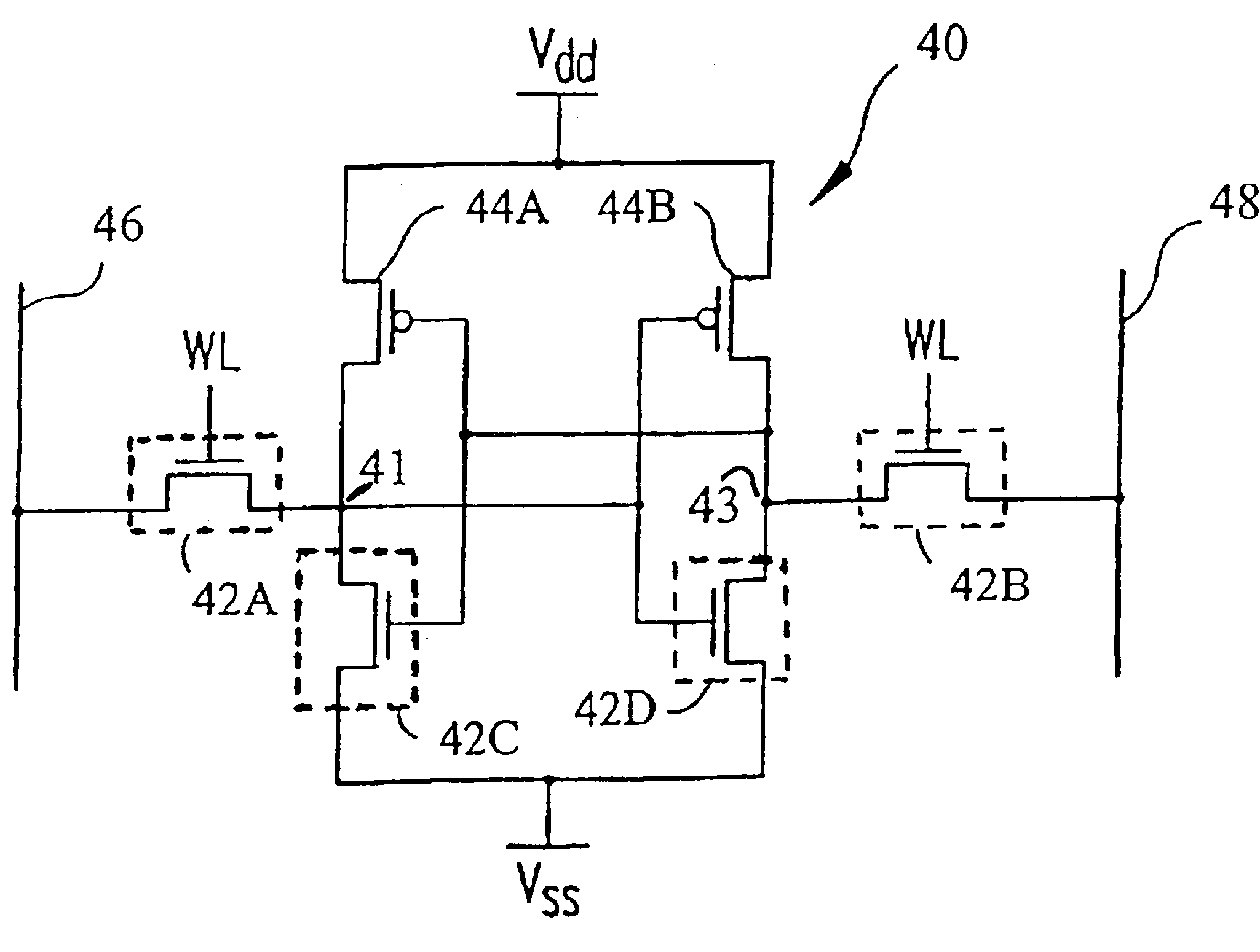
[0038]The exemplary embodiments of invention provide a SRAM cell design including a passgate device having a higher voltage threshold than a pull-down device. A threshold voltage of the passgate device is increased by ion implant with a critical mask. This facilitates forming a passgate device having a decreased layout area and thus reducing the overall size of a SRAM layout. The benefits of this design and method are minimizing access disturbances during read / write operations and decreasing a S...


PUM


Abstract

Methods for designing a 6T SRAM cell having greater stability and / or a smaller cell size are provided. A 6T SRAM cell has a pair access transistors (NFETs), a pair of pull-up transistors (PFETs), and a pair of pull-down transistors (NFETs), wherein the access transistors have a higher threshold voltage than the pull-down transistors, which enables the SRAM cell to effectively maintain a logic “0” during access of the cell thereby increasing the stability of the cell, especially for cells during “half select.” Further, a channel width of a pull-down transistor can be reduced thereby decreasing the size of a high performance six transistor SRAM cell without effecting cell the stability during access. And, by decreasing the cell size, the overall design layout of a chip may also be decreased.

Description

TECHNICAL FIELD OF THE INVENTION[0001]The present invention relates generally to digital logic circuits and more particularly, to the design of high performance static random access memories (SRAMs) built for increased stability.BACKGROUND[0002]Various factors that are considered for L1 cache memory include the size and performance of the type of memory used for implementing an L1 cache. In general, when L1 cache is embedded in a CPU (Central Processing Unit), its performance, e.g. access speed, must be compatible with CPU cycle time. Static random access memories (SRAMs) are primarily used for L1 cache memory as opposed to dynamic random access memories (DRAMs). Indeed, with respect to access speed, SRAM can provide access times of less than 1 ns, while the state-of-the-art DRAMs have access times ranging from 4 ns to 10 ns.[0003]On the other hand, SRAM cells are typically formed with 6 transistors (i.e., 6T Cell), whereas DRAM cells are formed with one transistor and one capacitor...

Claims


Application Information

Patent Timeline
Patent Type & Authority Patents(United States)
IPC IPC(8): G11C11/00G11C11/412H01L21/70H01L27/11H01L21/8244G11C11/41
CPCG11C11/412G11C5/02G11C5/06H10B10/00
Inventor CHAN, YUEN H.HSU, LOUIS L.JOSHI, RAJIV V.WONG, ROBERT CHI-FOON
Owner INTEL CORP
Why Eureka
Try Eureka