

Method of cleaning CVD device and cleaning device therefor
a technology of cvd and cleaning gas, which is applied in the direction of cleaning hollow objects, cleaning using liquids, manufacturing tools, etc., can solve the problems of cvd apparatus b>, contamination of semiconductor products, and inability to produce thin films of high quality, and achieve the effect of reducing cost and dissociation efficiency of cleaning gas
- Summary
- Abstract
- Description
- Claims
- Application Information
AI Technical Summary
Benefits of technology
Problems solved by technology
Method used
Image

Examples
example 1
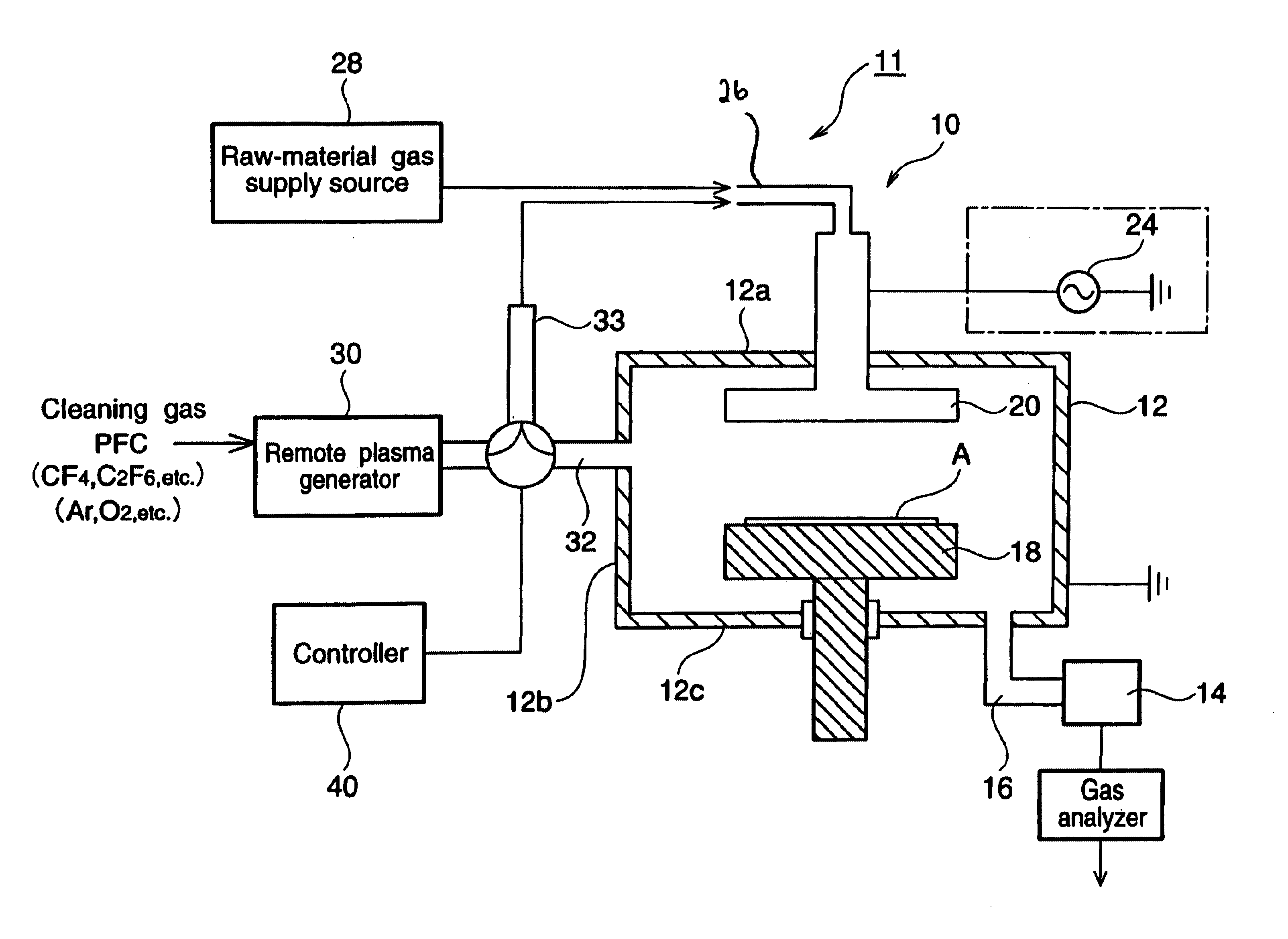
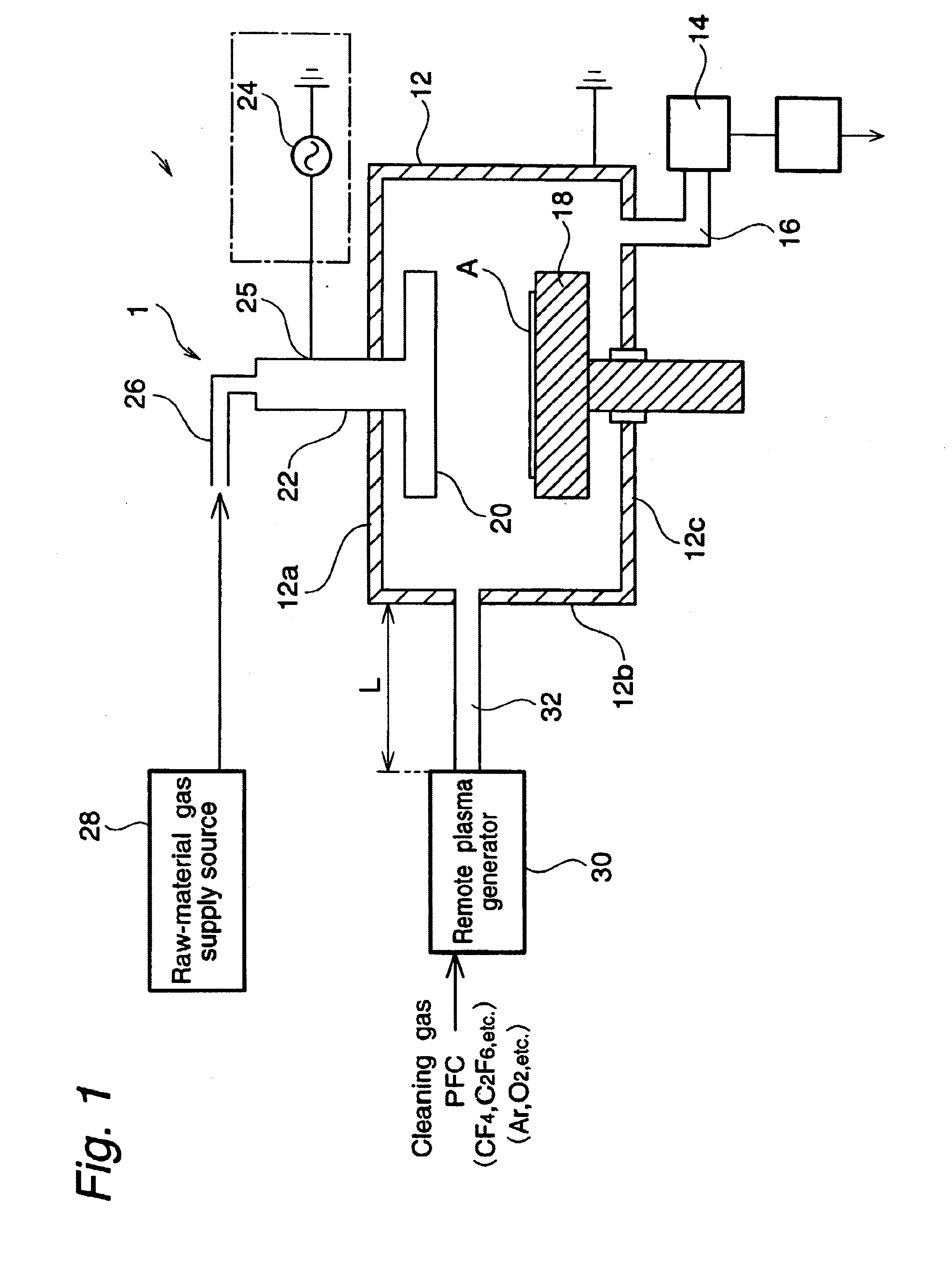
[0109]A base material (silicon substrate of 725 μm thickness and 200 mm diameter) was mounted on the lower electrode 18, using the CVD apparatus 10 of FIG. 1. As for raw-material reactive gas, specifically, monosilane gas 180 SCCM, ammonia 320 SCCM and N2 1 L / min were fed into the reaction chamber 12. The pressure inside the reaction chamber 12 was maintained at 320 Pa, and high frequency power of 520 W output from a 13.65 MHz high frequency power source was applied to the upper electrode 20. Under these conditions, film formation was performed for 40 sec so that a thin film of 7000 to 8000 Å was obtained.
[0110]After this film formation, the cleaning method of the present invention was carried out with the use of:
[0111]cleaning gas of 130 Pa pressure consisting of CF4 / Ar / O2 (gas flow rates 200 / 1600 / 400 (SCCM)), and
[0112]cleaning gas of 130 Pa pressure consisting of C2F6 / Ar / O2 (gas flow rates 100 / 1600 / 400 (SCCM)). The gas discharge amount and time required for chamber cleaning were m...
example 2
[0120]The cleaning method of the present invention was carried out with the use of cleaning gas consisting of C2F6 / Ar / O2 (gas flow rates 100 / 1600 / 400 (SCCM)) in the same manner as in Example 1, except that the cleaning pressure was varied within the range of 130 to 600 Pa, and the gas discharge amounts were measured. The results are shown in the graph of FIG. 7.
[0121]It is apparent from the results of FIG. 7 that the discharge amount of discharge gas resulting from cleaning can be lowered by increasing the pressure of cleaning gas during cleaning.
example 3
[0122]After each of various cleaning methods performed in the same manner as in the above Examples, long run film forming experiments were carried out under the same conditions as in Example 1 except that the pressure was 260 Pa. Further, as a comparative example, long run film forming experiments were also carried out in the case where no cleaning was performed.
[0123]After continuous film forming experiments, foreign matters (dirts) with a size of 1.01 μm or greater on the base material were inspected. The results are shown in the graph of FIG. 8.
[0124]As apparent from the graph of FIG. 8, with respect to the number of observed foreign matters as well, there is no marked difference between the remote plasma type cleaning method according to the present invention and the conventional parallel plate type plasma cleaning method.
[0125]In the present invention, the fluorinated cleaning gas containing a fluorocompound is converted to plasma by the remote plasma generator after the film f...
PUM
| Property | Measurement | Unit |
|---|---|---|
| distance | aaaaa | aaaaa |
| frequency | aaaaa | aaaaa |
| flow rate | aaaaa | aaaaa |
Abstract
Description
Claims
Application Information