Method for fabricating a memory device having reverse LDD

a memory device and reverse ldd technology, applied in the direction of semiconductor devices, electrical devices, transistors, etc., can solve the problems of reducing the efficiency affecting the performance of the memory device, and the threshold of the spec, so as to reduce the diffusion of the source and drain region, reduce the malfunction, and shorten the channel length

Inactive Publication Date: 2005-08-30
MONTEREY RES LLC
View PDF6 Cites 5 Cited by
  • Summary
  • Abstract
  • Description
  • Claims
  • Application Information

AI Technical Summary

Benefits of technology

[0009]The present invention provides a method for fabricating a semiconductor device that allows for adequate space at the core memory cell drain to form a contact and that reduces diffusion of the source and drain regions and shortening of channel length, thereby reducing malfunctions and improving performance in periphery transistors and core flash memory cells of the conventional semiconductor devices.
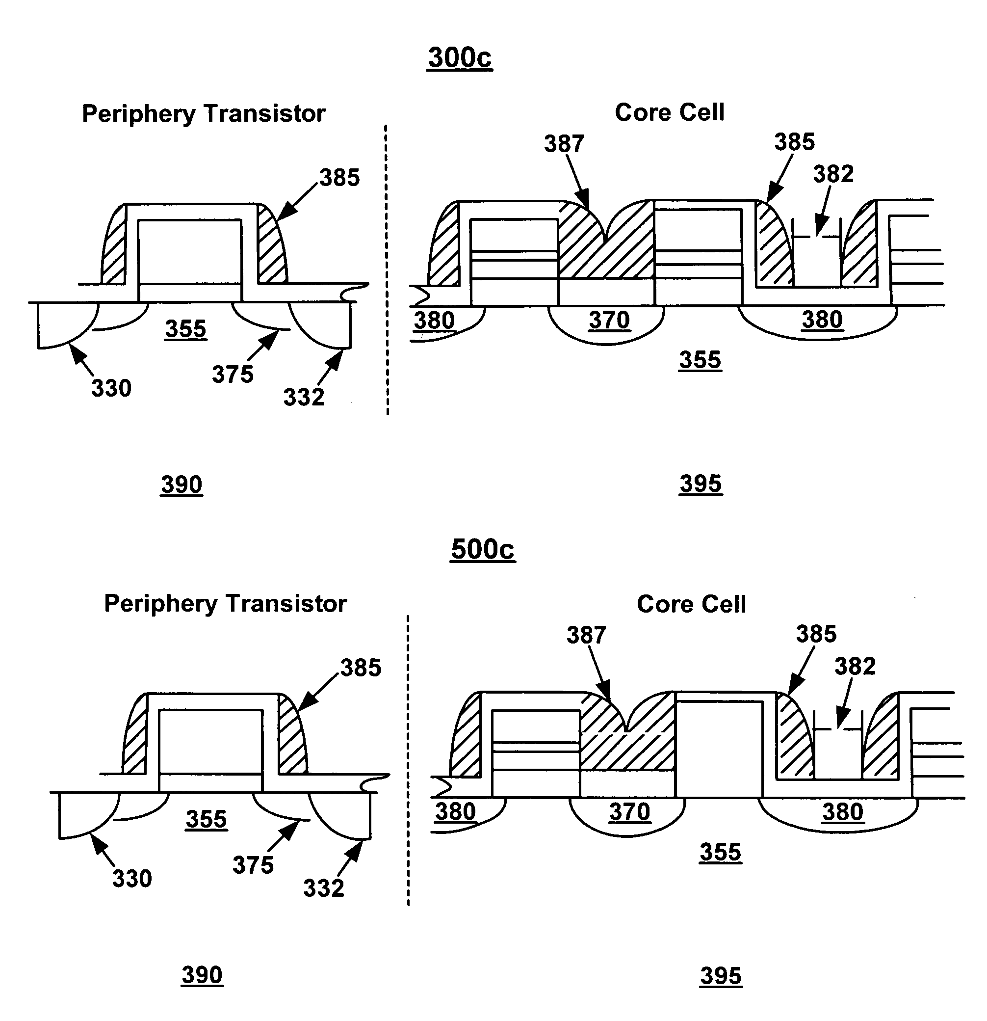
[0010]In various embodiments, the present invention presents a method for fabricating a semiconductor device. In one embodiment the method includes forming a source drain region in a periphery transistor, exhibiting a channel width between the source and drain regions suitable for operation at voltages greater than 10 volts. To eliminate diffusion of lightly doped drain regions resulting from a later formation of the source and drain regions, the lightly doped drain regions adjacent to the source and drain regions of the periphery transistor are formed after forming the source and drain regions of the periphery transistors. According to one embodiment, after forming the lightly doped drain regions in the periphery transistor, the method includes forming a source region and a drain region in a core memory cell, independent of forming the source and drain regions in the periphery transistor. The purpose of forming the core memory cell source and drain after the periphery transistor source and drain and lightly doped drain is to isolate the formation of a drain contact to the drain region of the core memory cell from the formation of the source and drain regions of the periphery transistor.

Problems solved by technology

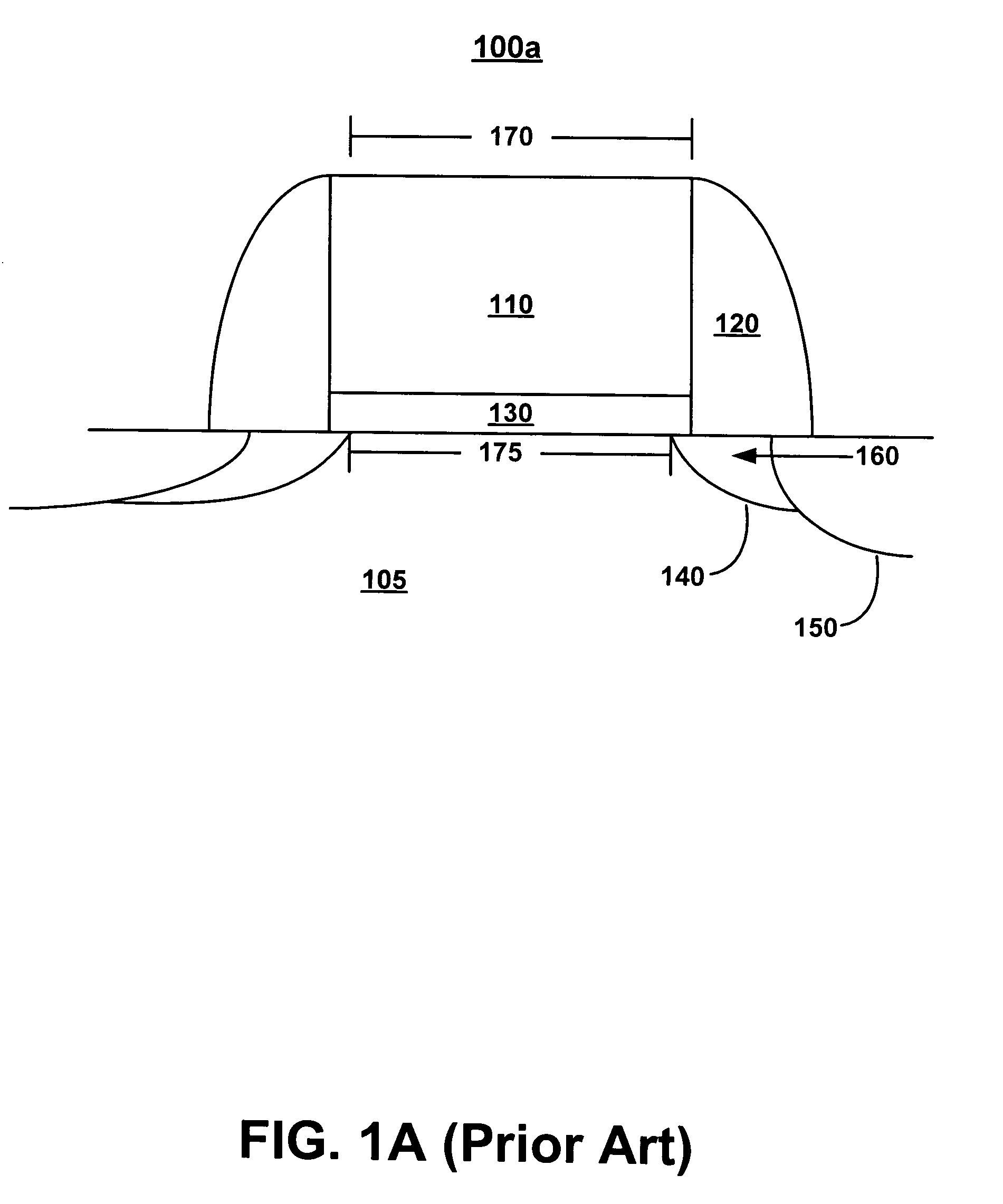
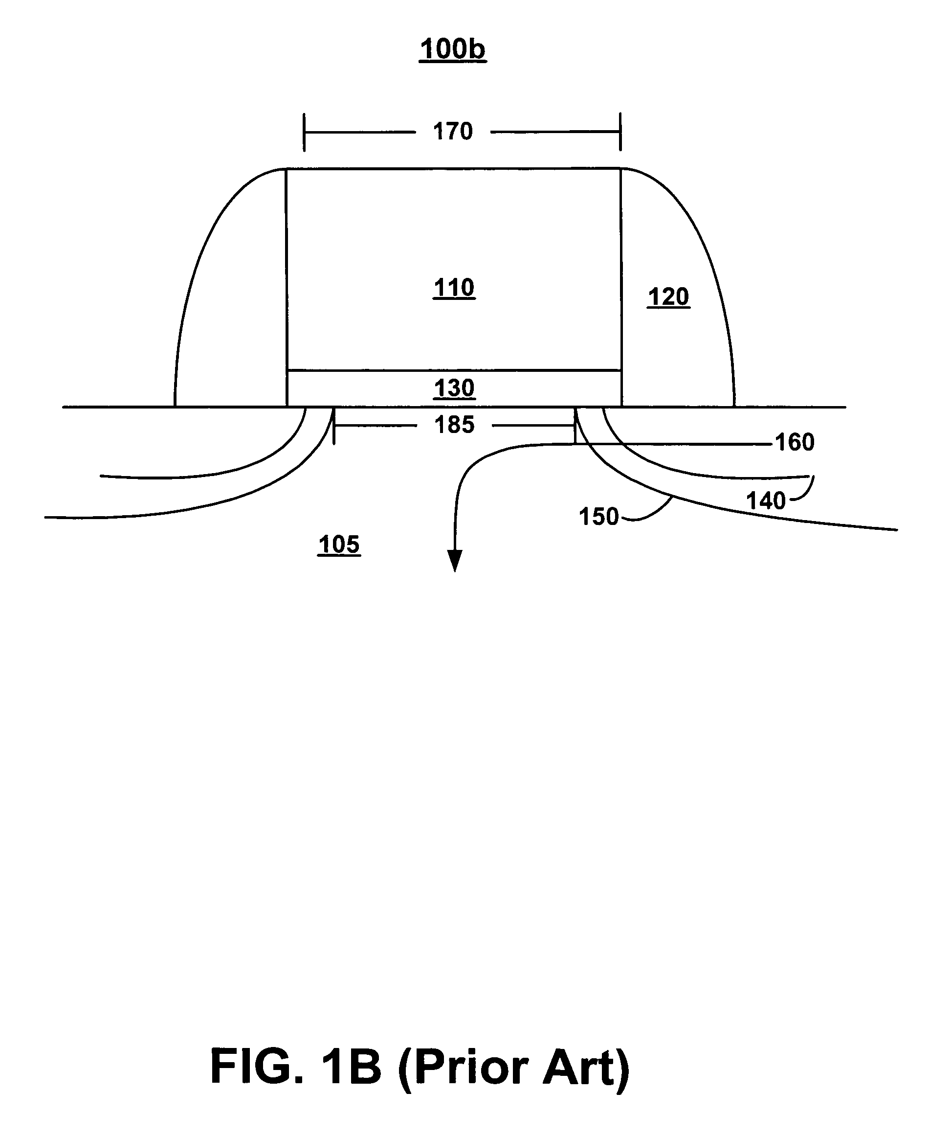
If effective channel length varies substantially from design channel length, the threshold voltage may be out of specification, causing a malfunction of the transistor.
This could put the threshold out of spec and cause a malfunction of transistor 100b.
As the state-of-the-art semiconductor devices become increasingly smaller, the conventional process for forming the silicon nitride layer that forms a common source area coupled to a source region of a transistor and the sidewalls at the drain region may become inadequate.

Method used


Image

  • Method for fabricating a memory device having reverse LDD
  • Method for fabricating a memory device having reverse LDD
  • Method for fabricating a memory device having reverse LDD

Examples


Embodiment Construction

[0027]Reference will now be made in detail to the preferred embodiments of the present invention, a reverse LDD method for fabricating a memory device. While the invention will be described in conjunction with the preferred embodiments, it will be understood that they are not intended to limit the invention to these embodiments. On the contrary, the invention is intended to cover alternatives, modifications and equivalents, which may be included within the spirit and scope of the invention as defined by the appended claims.

[0028]Furthermore, in the following detailed description of the present invention, numerous specific details are set forth in order to provide a thorough understanding of the present invention. However, it will be recognized by one of ordinary skill in the art that the present invention may be practiced without these specific details. In other instances, well known methods, procedures, components, and circuits have not been described in detail as not to unnecessar...


PUM


Abstract

A method for fabricating a semiconductor device. Specifically, a method that includes forming a source and drain region in a periphery transistor, exhibiting a channel width between the source and drain regions suitable for operation at predetermined voltages. After forming the source and drain regions, to eliminate diffusion of lightly doped drain regions resulting from a later formation of the source and drain regions, forming the lightly doped drain regions adjacent to the source and drain regions of the periphery transistor. After forming the lightly doped drain regions in the periphery transistor, the method includes forming a source region and a drain region in a core memory cell, independent of forming the source and drain regions in the periphery transistor.

Description

TECHNICAL FIELD[0001]The present invention relates to the field of semiconductor memory device fabrication. Specifically, embodiments of the present invention relate to changing the method of depositing the layers of the memory device to allow for thinner side-wall spacers without current breakdown and to reduce shortening of channel width.BACKGROUND ART[0002]Flash memory, which is sometimes called “flash ROM”, is a type of non-volatile memory that can be erased and reprogrammed in units of memory called blocks. It is a variation of electrically erasable programmable read-only memory which, unlike flash memory, is erased and rewritten at the byte level, which is slower than flash memory updating. Flash memory is used in digital cellular phones, digital cameras, LAN switches, PC Cards for notebook computers, digital set-up boxes, embedded controllers, and other devices.[0003]Flash memory gets its name from the organization of the microchip, which allows a section of the memory cells ...

Claims


Application Information

Patent Timeline
Patent Type & Authority Patents(United States)
IPC IPC(8): H01L21/02H01L21/336H01L21/8247H01L27/105
CPCH01L27/105H01L27/11526H01L27/11534H01L29/6656H01L29/6659H01L29/66825H10B41/43H10B41/40
Inventor OGAWA, HIROYUKISUN, YUHUI, ANGELA
Owner MONTEREY RES LLC
Why Eureka
Try Eureka