Transparent electrode, optoelectronic apparatus and devices

a transparent electrode and optoelectronic technology, applied in thermoelectric devices, instruments, optics, etc., can solve the problems of material doping to improve efficiency, reducing resistance to improve efficiency, and far from optimal, so as to achieve relatively inexpensive and large-scale production

Inactive Publication Date: 2005-08-30
AERIS CAPITAL SUSTAINABLE IP
View PDF22 Cites 240 Cited by
  • Summary
  • Abstract
  • Description
  • Claims
  • Application Information

AI Technical Summary

Benefits of technology

[0015]Embodiments of the present invention provide new and useful electrodes and devices that may be formed relatively inexpensively and on a large scale.

Problems solved by technology

These materials may or may not be doped to improve performance (e.g. reduce resistance to improve efficiency).
Thus one faces the problem of maximizing light transmission into the cell while minimizing the resistance of said electrode to efficiently (at low power loss) carry the collected current to the outside circuit or device.
Such approaches are still far from optimal as limited light transmission and residual resistances limit device efficiency and manufacturing is costly.
Furthermore, such approaches are not compatible with the use of organic PV cells.
Ichinose, in particular does not address applications involving organic PV cells.
It is known in the prior art that TCO materials, particularly where they act as anodes to extract and / or inject positive charge carriers, may not form good ohmic or near-ohmic contacts with organic p-type materials such as those employed in organic or partly-organic solar cells.
Furthermore, organic or partly organic solar cells are often more sensitive to ‘process conditions’.
For example, depositing a TCO layer (e.g. via the typical sputtering processes or even reactive sputtering processes that create UV and / or plasma conditions) can damage the organic layers such that cells may, for example have electrical shorts.
Furthermore, TCO deposition processes typically employ vacuum-coating steps that are difficult and costly, even in a web-based roll-to-roll process.
Unfortunately, after processing such as coating and drying, such conductive polymer films have sheet resistances significantly higher than TCOs; e.g., about 200 Ohms / square.
Because of this, the resistive power loss would be far too high.
Thus, pure conductive polymer transparent electrodes are unacceptable for PV approaches.

Method used


Image

  • Transparent electrode, optoelectronic apparatus and devices
  • Transparent electrode, optoelectronic apparatus and devices
  • Transparent electrode, optoelectronic apparatus and devices

Examples


Embodiment Construction

Contents

[0027]I. Glossary[0028]II. General Overview[0029]III. Apparatus Using Transparent Conducting Electrodes[0030]IV. Optoelectronic Devices using Transparent Conducting Electrodes[0031]V. Fabrication of Transparent Conducting Electrodes[0032]VI. Fabrication of Apparatus, and Devices[0033]VII. Alternative Embodiments[0034]VIII. Conclusion

I. Glossary

[0035]The following terms are intended to have the following general meanings as they are used herein:

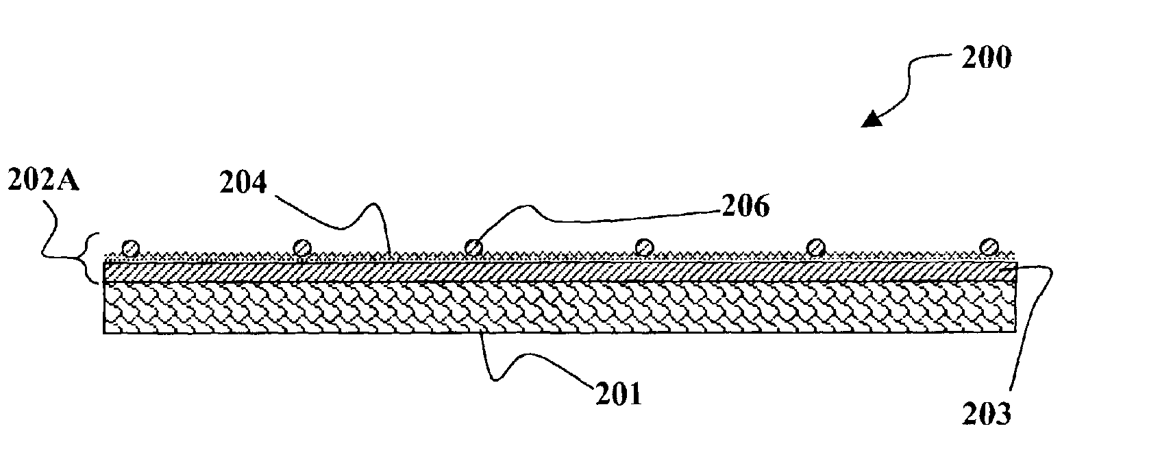
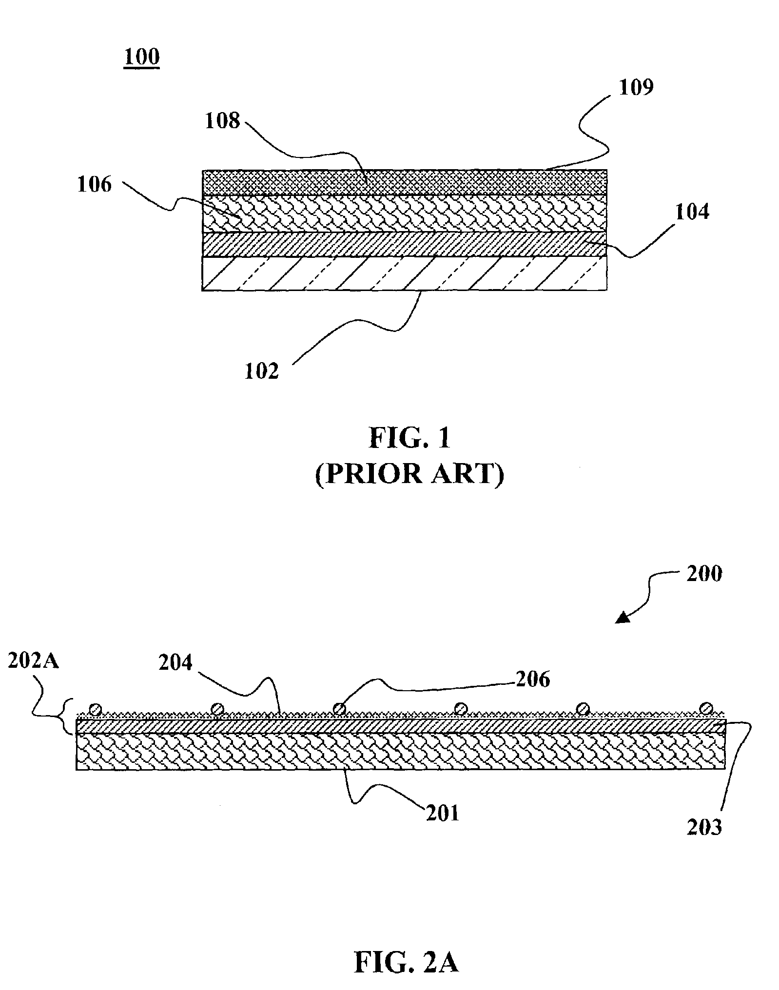
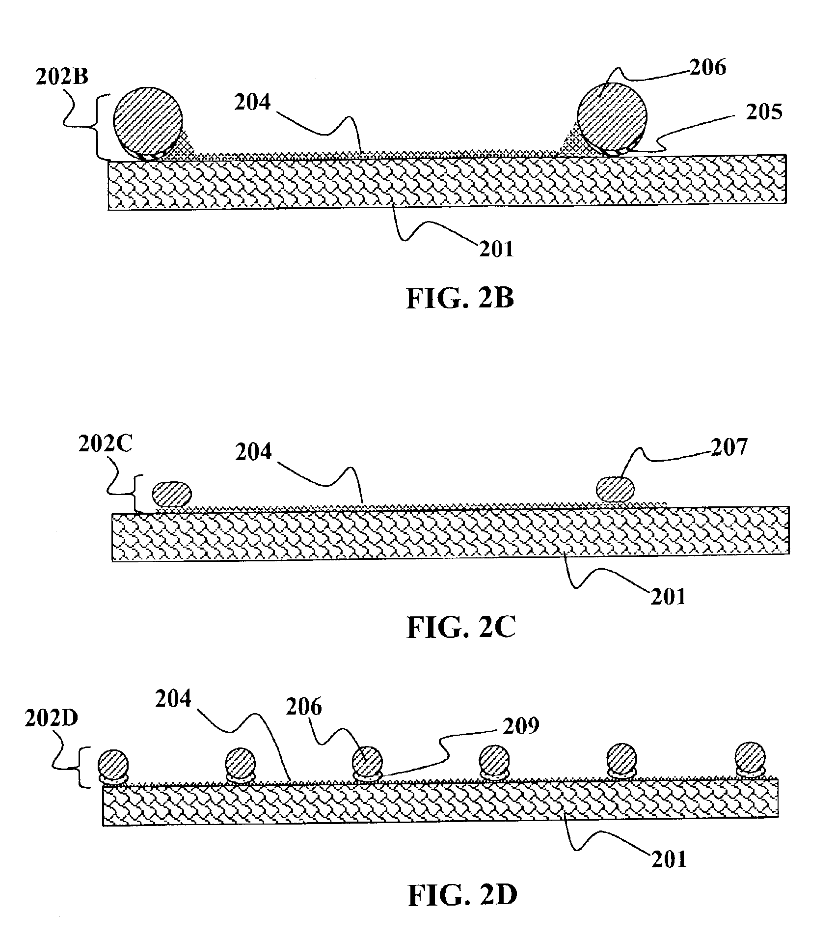
[0036]Device: An assembly or sub-assembly having one or more layers of material.

[0037]Semiconductor: As used herein, semiconductor generally refers to a material characterized by an electronic bandgap typically between about 0.5 eV and about 3.5 eV.

[0038]Hole-Acceptor, Electron-Acceptor: In the case of semiconductor materials, hole-acceptor and electron-acceptor are relative terms for describing charge transfer between two materials. For two semiconductor materials wherein a first material has a valence band edge or highest occupied mo...


PUM

PropertyMeasurementUnit
diametersaaaaaaaaaa
diametersaaaaaaaaaa
diametersaaaaaaaaaa

Abstract

Transparent conductive electrodes, optoelectronic apparatus, optoelectronic devices and methods for making such electrodes, apparatus and devices are disclosed. The transparent conducting electrode (TCE) includes a layer of transparent electrically conducting polymer material and an array of electrically conductive wires distributed across the layer of transparent electrically conducting polymer material. The TCE may be made by distributing an array of conductive wires across a conductive polymer layer and attaching polymer layer to the wire array. An optoelectronic apparatus may comprise an active layer in electrical contact with the TCE. An optoelectronic device may incorporate an active layer disposed between two electrodes, at least one of which is the TCE. An optoelectronic device may be made by disposing an active layer between a base electrode and a TCE and attaching all three together.

Description

CROSS-REFERENCE TO RELATED APPLICATIONS[0001]This application is related to commonly assigned copending U.S. patent applications Ser. Nos. 10 / 290,119, 10 / 303,665, 10 / 319,406 and 10 / 338,079, all of which are incorporated herein by reference.FIELD OF THE INVENTION[0002]This invention generally relates to optoelectronic devices and more particularly to transparent conducting electrodes for such devices.BACKGROUND OF THE INVENTION[0003]Optoelectronic devices interact with radiation and electric current. Such devices can be light-emitting devices that produce radiation as a result of an applied electric voltage / current or photovoltaic devices that produce an electric voltage / current as a result of applied radiation. Photovoltaic (PV) cells / devices typically employ a substrate or carrier (wafer, film, foil, etc.), a bottom electrode, one or more layers of PV material and a top electrode. Either the bottom electrode or the top electrode may be the anode and the opposite the cathode and vic...

Claims


Application Information

Patent Timeline
Patent Type & Authority Patents(United States)
IPC IPC(8): H01L31/0224H01L31/00H01L31/04H01L31/18H01L33/42
CPCG02F1/155H01L31/022425H01L31/022466H01L31/1884H01L33/42H01L51/442Y02E10/50H01L2924/0002H01L2924/00H10K30/82
Inventor PICHLER, KARL
Owner AERIS CAPITAL SUSTAINABLE IP
Why Eureka
Try Eureka