Insulated-gate field-effect transistor, method of fabricating same, and semiconductor device employing same

a field-effect transistor and insulating gate technology, applied in the field of insulated gate field-effect transistors, can solve the problems of inability to sufficiently reduce the thickness of the layer upon the insulator layer, difficult to achieve high performance through downsizing, and the p-type transistor is more susceptible to punching through, etc., to achieve short gate length, high mobility, and easy fabrication

Inactive Publication Date: 2005-08-30
RENESAS ELECTRONICS CORP
View PDF7 Cites 102 Cited by
  • Summary
  • Abstract
  • Description
  • Claims
  • Application Information

AI Technical Summary

Benefits of technology

[0009]The present invention has been developed to resolve various problems of the conventional technology, and is intended to provide an insulated-gate field-effect transistor having high mobility and a short gate length. Further, another object of the present invention is to provide a double-gate transistor that can be fabricated with ease. Still another object of the present invention is to provide a new semiconductor device by forming transistors having different characteristics on the same substrate with ease.

Problems solved by technology

However, when the gate of a transistor is e.g., a size less than 50 nm, it has become extremely difficult to achieve high performance through downsizing only.
With the conventional strained SOI, it has been impossible to sufficiently reduce the thickness of the layer upon the insulator layer because of the need for presence of the silicon germanium layer.
Accordingly, there has occurred a problem that a p-type transistor is more susceptible to occurrence of punch-through.
Furthermore, one drawback of substrates employed previously is that they have required a fabrication process using a special method of bonding, among other things, and consequently, fabrication cost thereof becomes higher in comparison with a conventional Si or SOI substrate.

Method used


Image

  • Insulated-gate field-effect transistor, method of fabricating same, and semiconductor device employing same
  • Insulated-gate field-effect transistor, method of fabricating same, and semiconductor device employing same
  • Insulated-gate field-effect transistor, method of fabricating same, and semiconductor device employing same

Examples


embodiment 1

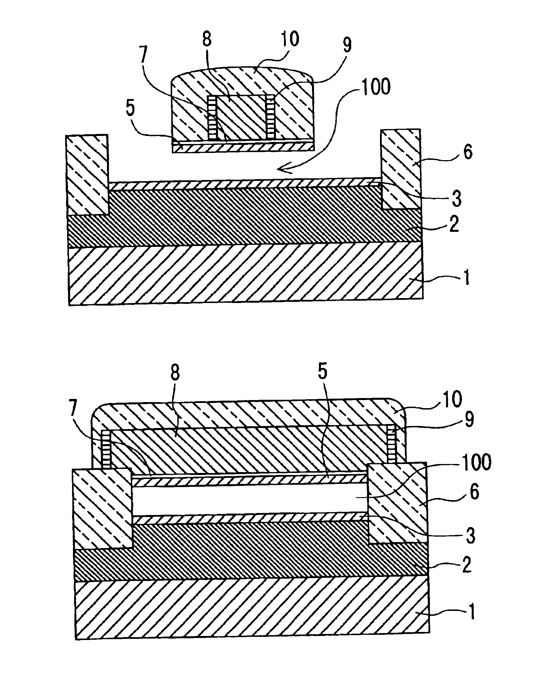
[0089]Embodiment 1 is concerned with a method of fabricating an insulated-gate field-effect transistor for which a novel planar configuration is devised for removal of a portion of a silicon germanium layer, directly underneath a strained silicon layer.

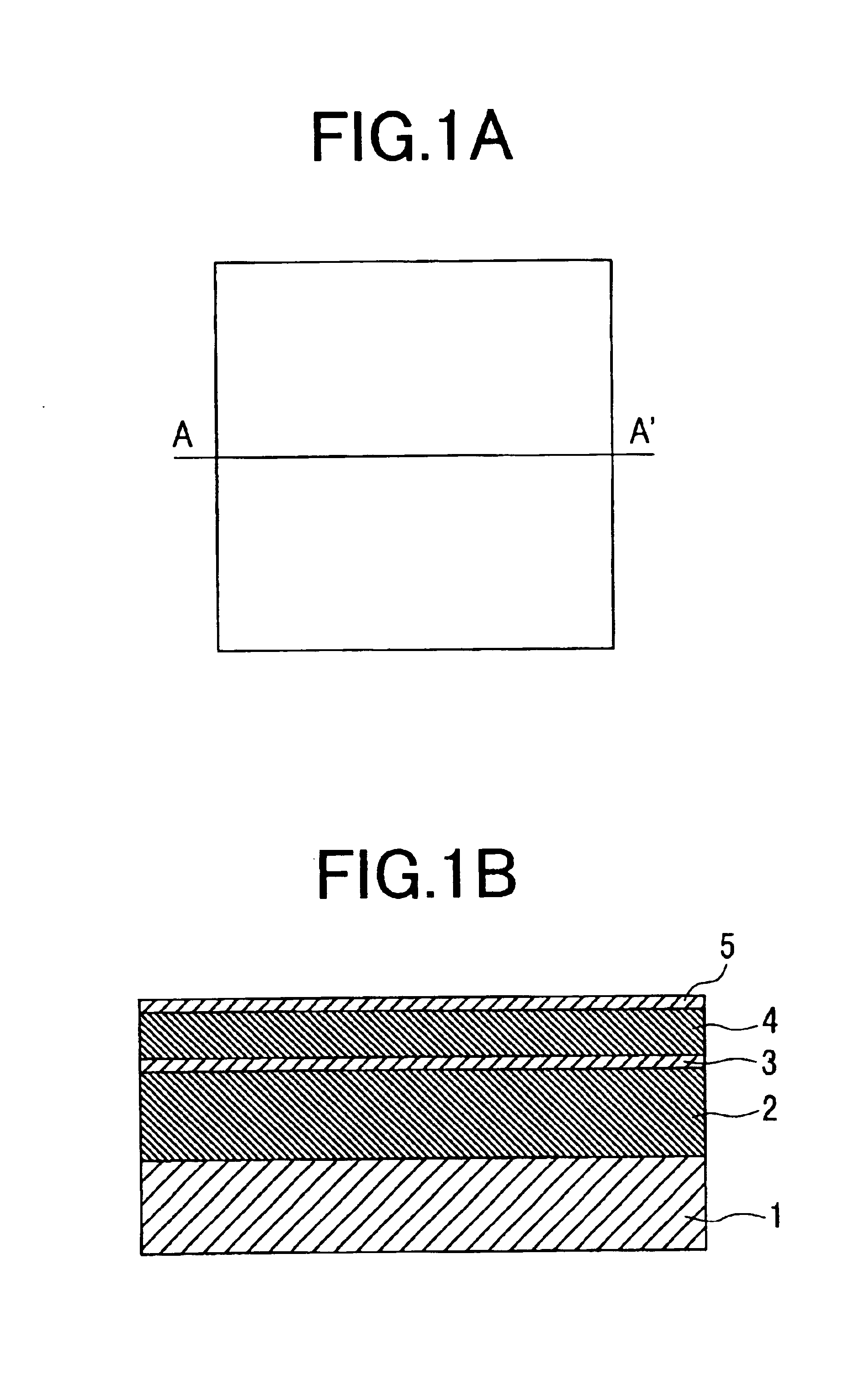
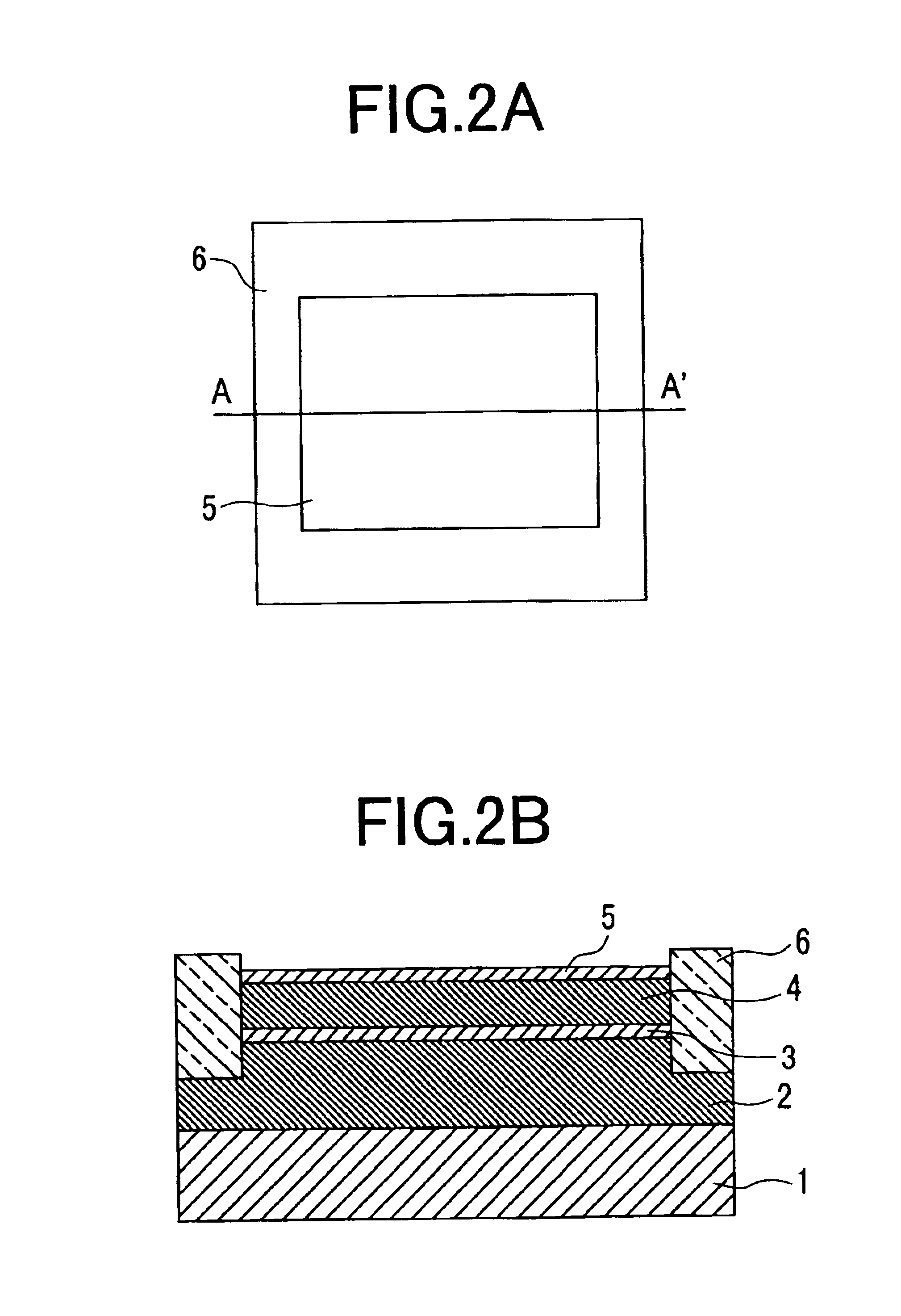
[0090]FIGS. 1 through 9 are schematic illustrations showing a semiconductor device in the order of steps of the method of fabricating the same according to the present embodiment. FIG. 1 shows a strained silicon / strain-relaxed silicon germanium substrate by way of example. FIG. 1A is a plan view of the substrate and FIG. 1B is a sectional view taken on line A-A′ in FIG. 1A. Suffix “A” of FIGS. 1 through 9, respectively, indicates a plan view of a base body, suffix “B” is a sectional view taken on line A-A′ in “A” of the respective figures, and suffix “C” is a sectional view taken on line B-B′ in “A” of the respective figures. Only FIGS. 5 through 9 are provided with suffix “C”.

[0091]The strained silicon / strain-relaxed silicon germaniu...

embodiment 2

[0105]Embodiment 2 differs from Embodiment 1 in that use of an SOI substrate is substituted for use of the substrate according to Embodiment 1.

[0106]The SOI substrate has a structure, as shown in a sectional view of FIG. 10, wherein an embedded insulating film 13, a strain-relaxed silicon germanium layer 4, and a strained silicon layer 5 are combined in that order on a silicon substrate 1. The silicon substrate 1 is intended only to support those film deposited thereon, and may be made of, for example, quartz, an inorganic oxide ceramic, and so forth, other than silicon.

[0107]With the present embodiment, although the substrate is changed, other steps of a fabrication method can be executed in the same way as those for Embodiment 1. Further, the etching of the silicon germanium layer 4 according to Embodiment 1, as shown with reference to FIG. 6, is stopped at the embedded insulating film 13. Since etch selectivity of silicon germanium to an oxide film is higher than that of silicon ...

embodiment 3

[0108]Embodiment 3 is concerned with a transistor having strained silicon channels of a fin-shaped structure.

[0109]FIG. 12 is a sectional view of a substrate according to the present embodiment. FIGS. 13 and 14 and FIGS. 19 through 29 are schematic illustrations of a device in a fabrication process according to the present embodiment. Suffix “A” of the respective figures indicates a plan view of the device, suffix “B” a sectional view taken on line A-A′ of the respective figures with A, and suffix “C” a sectional view taken on line B-B′ of the respective figures with suffice “A”. FIGS. 24 and 28 are perspective views of the device in the fabrication process.

[0110]FIGS. 15 through 18 are schematic views for illustrating features of a strained silicon layer. FIGS. 15 and 16 are sectional views showing the direction of tensile strain by way of example when a strained silicon layer 5 is grown on a silicon germanium layer 4 while FIGS. 17 and 18 are perspective views showing a relationsh...


PUM


Abstract

With the invention, it is possible to avoid deterioration in short-channel characteristics, caused by a silicon germanium layer coming into contact with the channel of a strained SOI transistor. Further, it is possible to fabricate a double-gate type of strained SOI transistor or to implement mixedly mounting the strained SOI transistor and a conventional silicon or SOI transistor on the same wafer. According to the invention, for example, a strained silicon layer is grown on a strain-relaxed silicon germanium layer, and subsequently, portions of the silicon germanium layer are removed, thereby constituting a channel layer in the strained silicon layer.

Description

BACKGROUND OF THE INVENTION[0001]1. Field of the Invention[0002]The present invention relates to an insulated-gate field-effect transistor having high-mobility channel and a short gate length, and a method of fabricating the same. Further, the present invention is concerned with a semiconductor device employing the insulated-gate field-effect transistors. The transistor according to the present invention is useful when applied to a semiconductor device for use in an electronic circuit including a logic circuit, an analog circuit, and so on, particularly, in a field where high speed and low power consumption are required.[0003]2. Description of the Related Art[0004]In the case of a silicon semiconductor device, particularly, a field effect transistor, larger scale integration of a circuit has so far been realized and higher performance thereof has been obtained by downsizing the device. However, when the gate of a transistor is e.g., a size less than 50 nm, it has become extremely di...

Claims


Application Information

Patent Timeline
Patent Type & Authority Patents(United States)
IPC IPC(8): H01L21/02H01L29/786H01L21/336H01L29/10H01L29/02H01L29/80H01L29/66H01L21/20H01L21/764H01L21/762H01L21/8234H01L27/08H01L27/088H01L27/12
CPCH01L29/1054H01L29/66795H01L29/7842H01L29/785H01L29/78648H01L29/78687H01L29/802
Inventor SUGII, NOBUYUKIOHNISHI, KAZUHIROWASHIO, KATSUYOSHI
Owner RENESAS ELECTRONICS CORP
Why Eureka
Try Eureka