

Film forming apparatus and method of manufacturing light emitting device
a technology of film forming and film forming equipment, which is applied in the direction of discharge tube luminescnet screen, discharge tube/lamp details, electric discharge lamps, etc., can solve the problems of difficult processing of a large number of substrates, and achieve the effect of simplifying the overall system and easy maintenan
- Summary
- Abstract
- Description
- Claims
- Application Information
AI Technical Summary
Benefits of technology
Problems solved by technology
Method used
Image

Examples
embodiment 1
[Embodiment 1]
[0079]Here, a method of simultaneously forming, on the same substrate, a pixel portion and TFTs (n-channel TFT and p-channel TFT) of a driver circuit provided in the periphery of the pixel portion, is described in detail with FIGS. 3A to 5B.
[0080]First, in this embodiment, a substrate 300 is used, which is made of glass such as barium borosilicate glass or aluminum borosilicate, represented by such as Corning #7059 glass and #1737 glass. Note that, as the substrate 300, there is no limitation provided that it is a substrate with transmittance, and a quartz substrate may be used. A plastic substrate with heat resistance to a process temperature of this embodiment may also be used.
[0081]Then, a base film 301 formed of an insulating film such as a silicon oxide film, a silicon nitride film or a silicon nitride oxide film is formed on the substrate 300. In this embodiment, a two-layer structure is used as the base film 301. However, a single-layer film or a lamination stru...
embodiment 2
[Embodiment 2]
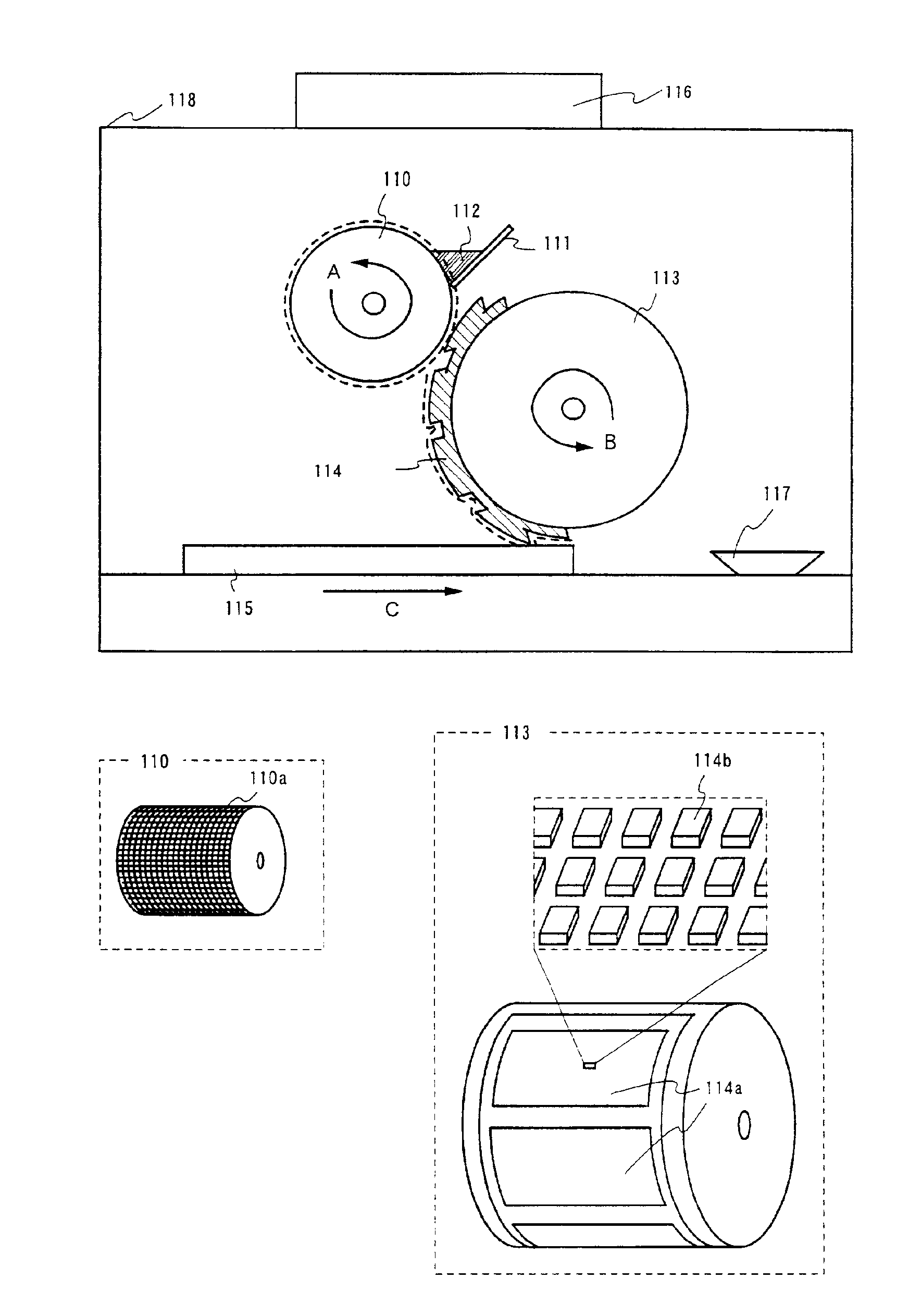
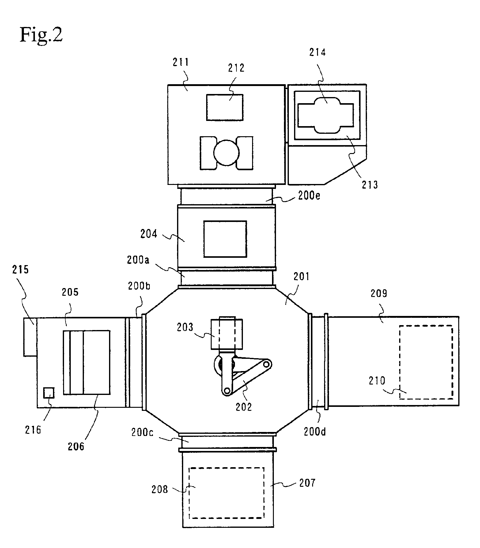
[0137]Embodiment 1 shows a process from forming an EL layer through sealing an EL element with the use of a multi-chamber film forming apparatus. Described in Embodiment 2 with reference to FIGS. 7A and 7B is how to conduct a series of processing from forming the EL layer through sealing the EL element using an in-line film forming apparatus.
[0138]FIG. 7A is a top view of the in-line film forming apparatus and FIG. 7B is a side view thereof. Reference symbol 701 denotes a loader unit (transfer unit) for substrates to be processed. As described in Embodiment 1, each substrate to be processed has finished up through forming an anode (or a cathode) of an EL element before setting in the loader unit 701.
[0139]An EL layer is printed on the substrate in a printing chamber 702 provided with a letterpress printing device. The printing chamber 702 is composed of an ink tank 703, a doctor bar 704, an anilox roll 705, and a printing roll 706 as shown in FIG. 7B. When an EL formin...
embodiment 3
[Embodiment 3]
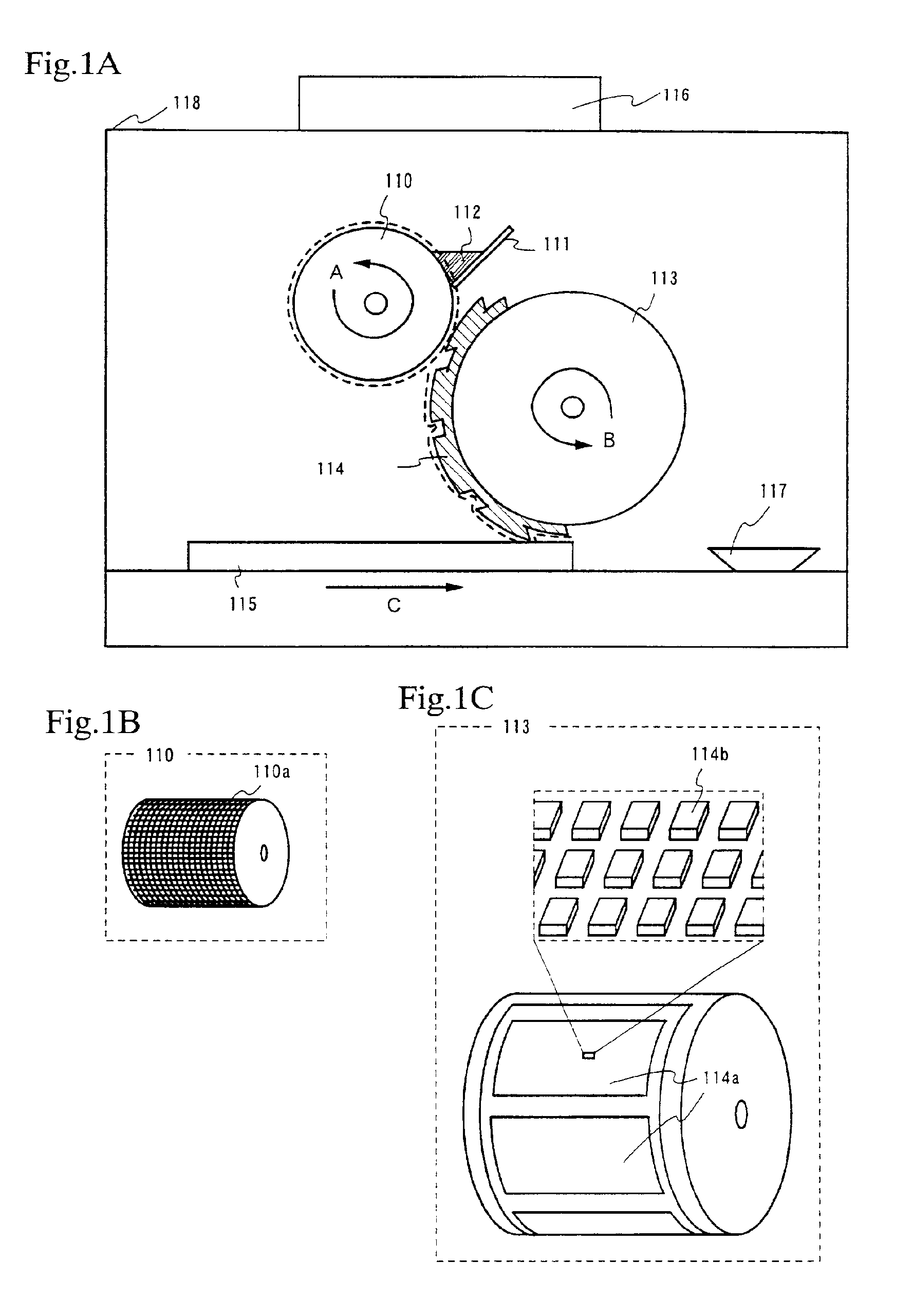
[0155]This embodiment gives an explanation on how to form a multi-color EL layer by the letterpress printing method shown in Embodiment 1. In FIG. 8A, reference symbol 801 denotes a printing roll provided in a printing chamber. The surface of the printing roll 801 is provided with a letterpress plate formed by etching or the like. The letterpress plate has plural pixel portion patterns 802 in order to form plural sheets of light emitting device on a single substrate.
[0156]Looking at the enlarged view of the pixel portion patterns 802, each pattern has convex 803 at positions corresponding to positions of a plurality of pixels. The configuration of the convex 803 is different for each color since a plurality of colors are to be obtained by letterpress in this embodiment.
[0157]For instance, when an EL forming material is printed using convex 803a shown in FIG. 8B, the pixel portion of first color pixels are formed as illustrated by the solid line regions in FIG. 8B.
[0158...
PUM
| Property | Measurement | Unit |
|---|---|---|
| Pressure | aaaaa | aaaaa |
| Pressure | aaaaa | aaaaa |
| Luminescence | aaaaa | aaaaa |
Abstract
Description
Claims
Application Information