Process for low temperature atomic layer deposition of RH

a technology of atomic layer deposition and rh, which is applied in the direction of chemical vapor deposition coating, coating, transistor, etc., can solve the problems of poor conformality of rf sputtering process and damage to pores or holes in thin films, and achieve good step coverage and good step coverage

Inactive Publication Date: 2005-09-13
MICRON TECH INC
View PDF10 Cites 14 Cited by
  • Summary
  • Abstract
  • Description
  • Claims
  • Application Information

AI Technical Summary

Benefits of technology

[0008]The present invention provides a novel method for the formation of rhodium films with good step coverage which may be used as top and / or lower plate electrodes for a capacitor. Rhodium films are formed by a low temperature atomic layer deposition technique using a rhodium gas precursor followed by an oxygen exposure. The invention provides, therefore, a method for forming smooth and continuous rhodium films which also have good step coverage.

Problems solved by technology

These technologies, however, have some disadvantages.
For example, the RF sputtering process yields poor conformality, while the spin deposition of thin films is a complex process, which generally involves two steps: an initial step of spinning a stabilized liquid source on a substrate usually performed in an open environment, which undesirably allows the liquid to absorb impurities and moisture from the environment; and a second drying step, during which evaporation of organic precursors from the liquid may leave damaging pores or holes in the thin film.
The use of platinum as the material of choice for capacitor electrodes poses, however, problems.
One of them arises from the difficulty of etching and / or polishing platinum.
Although the CVD processing technologies afford good step coverage, as the geometries of the future generations of semiconductors become extremely aggressive, these processing technologies will not be able to afford better step coverage, that is a high degree of thickness and / or uniformity control over a complex topology for thin films of such future generation of semiconductors.

Method used


Image

  • Process for low temperature atomic layer deposition of RH
  • Process for low temperature atomic layer deposition of RH
  • Process for low temperature atomic layer deposition of RH

Examples


example

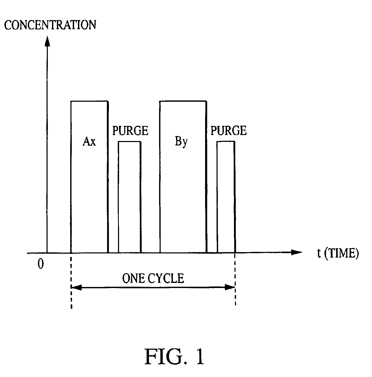
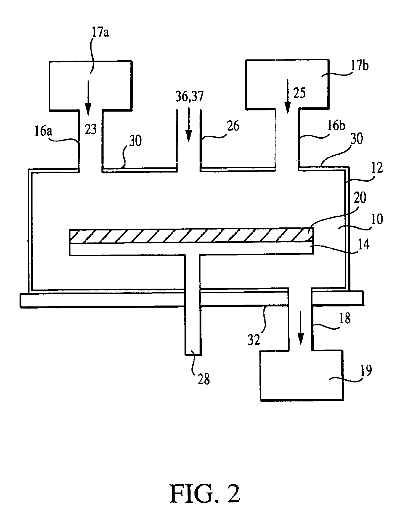
[0052]first precursor: 5 sccm dicarbonyl cyclopentadienyl rhodium [CpRh(CO2)] at about 100° C. and for about 5 seconds[0053]first purge gas: 50 sccm He for about 5 seconds[0054]second precursor: 50 sccm O2 for about 5 seconds[0055]second purge gas: 50 sccm He for about 5 seconds

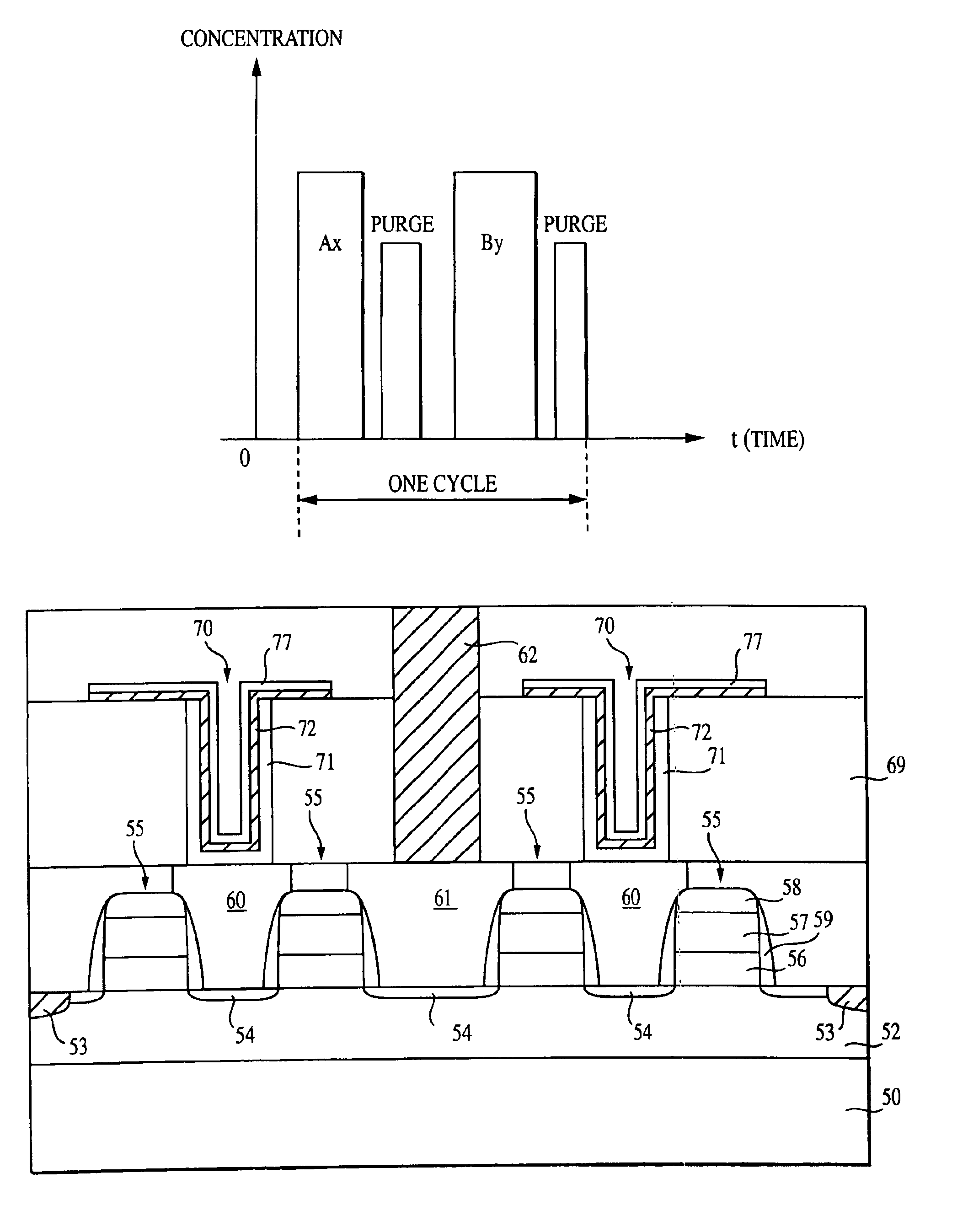
[0056]Although the invention has been described with reference to the formation of an upper rhodium plate of an MIM capacitor, the invention is not limited to the above embodiments. Thus, the invention contemplates the formation of high quality rhodium films with good step coverage that can be used in a variety of IC structures, for example as seed layers for electroplating processes, as fuse elements or as bond pads, among many others.

[0057]The MIM capacitor 70 of FIG. 4 including the rhodium film 77 formed according to a method of the present invention could further be part of a memory device of a typical processor based system, which is illustrated generally at 400 in FIG. 6. A processor system, such as a ...


PUM

PropertyMeasurementUnit
temperatureaaaaaaaaaa
thicknessaaaaaaaaaa

Abstract

A method for the formation of rhodium films with good step coverage is disclosed. Rhodium films are formed by a low temperature atomic layer deposition technique using a first gas of rhodium group metal precursor followed by an oxygen exposure. The invention provides, therefore, a method for forming smooth and continuous rhodium films which also have good step coverage and a reduced carbon content.

Description

[0001]This application is a divisional of application Ser. No. 09 / 884,997, filed on Jun. 21, 2001, now U.S. Pat. No. 6,656,835, which is incorporated herein by reference.FIELD OF THE INVENTION[0002]The present invention relates to the field of semiconductor integrated circuits and, in particular, to a novel method for forming high quality rhodium (Rh) films.BACKGROUND OF THE INVENTION[0003]Thin film technology in the semiconductor industry requires thin deposition layers, increased step coverage, large production yields, and high productivity, as well as sophisticated technology and equipment for coating substrates used in the fabrication of various devices. For example, process control and uniform film deposition directly affect packing densities for memories that are available on a single chip or device. Thus, the decreasing dimensions of devices and the increasing density of integration in microelectronics circuits require greater uniformity and process control with respect to la...

Claims


Application Information

Patent Timeline
Patent Type & Authority Patents(United States)
IPC IPC(8): C23C16/18C23C16/04C23C16/455H01L21/02C23C16/44H01L27/108
CPCC23C16/045C23C16/16C23C16/18C23C16/4401C23C16/45553H01L27/10852H01L28/60H01L28/65H01L27/10811H01L28/55H10B12/312H10B12/033
Inventor MARSH, EUGENE P.UHLENBROCK, STEFAN
Owner MICRON TECH INC
Why Eureka
Try Eureka