Aluminum-beryllium alloys for air bridges

a technology of air bridge and alloy, which is applied in the direction of solid-state devices, semiconductor devices, semiconductor/solid-state device details, etc., can solve the problems of increased capacitance between wires, cross talk, waste of power, etc., and achieves more rigidity and electrical resistance, the effect of superior rigidity and comparable electrical resistan

Inactive Publication Date: 2005-09-13
CONVERSANT INTPROP MANAGEMENT INC
View PDF52 Cites 4 Cited by
  • Summary
  • Abstract
  • Description
  • Claims
  • Application Information

AI Technical Summary

Benefits of technology

[0010]To address these and other needs, the inventor has developed new aluminum-beryllium alloys which, compared to the conventional aluminum alloy, have superior rigidity and comparable electrical resistance. Specifically, one alloy within the scope of the invention contains 25 weight-percent beryllium and 0.5 weight-percent copper, with the balance being aluminum and reasonably unavoidable impurities. This alloy provides an elastic-modulus-to-density (E / ρ) ratio (a measure of rigidity) of 40.9 Gpam3 / Mg and an electrical resistance of 31.3 nano-ohm-meters (nΩm). In contrast, a conventional aluminum alloy has an elastic-modulus-to-density ratio of about 25.4 GPam3 / Mg and an electrical resistance of 28.2 nano-ohm-meters. Thus, this aluminum-beryllium alloy is about 60 percent more rigid with only about 10 percent more electrical resistance than the conventional aluminum alloy. Moreover, all other factors being equal, this aluminum-beryllium alloy facilitates construction of air bridges that are 40-percent longer than bridges using the conventional aluminum alloy. Thus, the present invention promotes integrated circuits with superior speed and efficiency.

Problems solved by technology

Unfortunately, this closer spacing has increased capacitance between wires.
Increased capacitance not only causes cross talk—undesirable signal mixing between adjacent wires—but also wastes power and slows response of integrated circuits to electrical signals.
In fact, there are very few, if any, practical insulators with a lower dielectric constant.
Unfortunately, conventional fabrication techniques are limited to making short air bridges, typically with unsupported, or free-span, lengths about 1 millimeter long (assuming a 500-nanometer thickness and a maximum allowable sag of 250 nanometers).
The air bridges must be kept short because the typical aluminum alloy used to make air-bridge conductors is too supple and the conductors sag in the middle, sometimes forming short circuits with other conductors or even breaking.
However, most metals that would enhance rigidity of the typical aluminum alloy also substantially increase its density (mass per unit volume) or its electrical resistance, generally rendering the resulting wires too heavy or too electrically resistive to benefit air-bridge applications.

Method used


Image

  • Aluminum-beryllium alloys for air bridges
  • Aluminum-beryllium alloys for air bridges
  • Aluminum-beryllium alloys for air bridges

Examples


Embodiment Construction

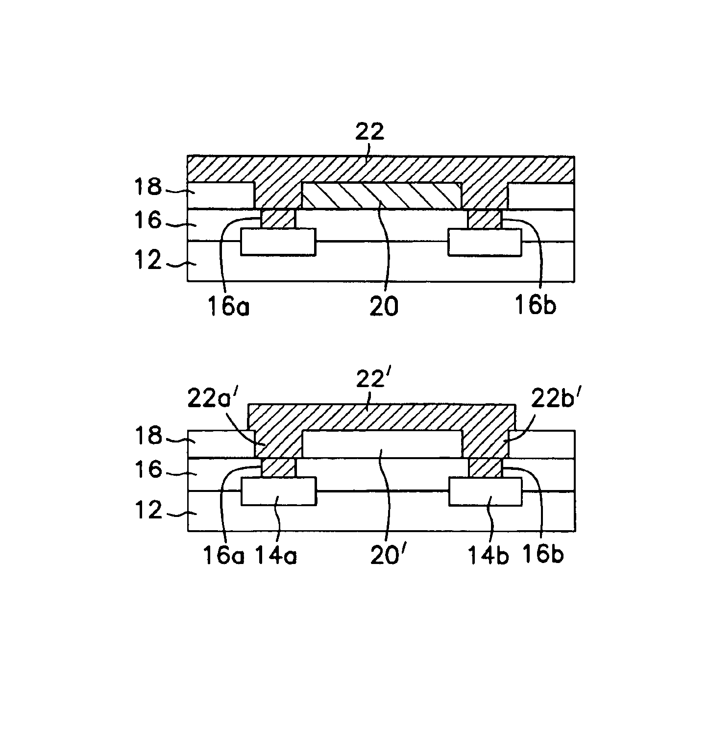
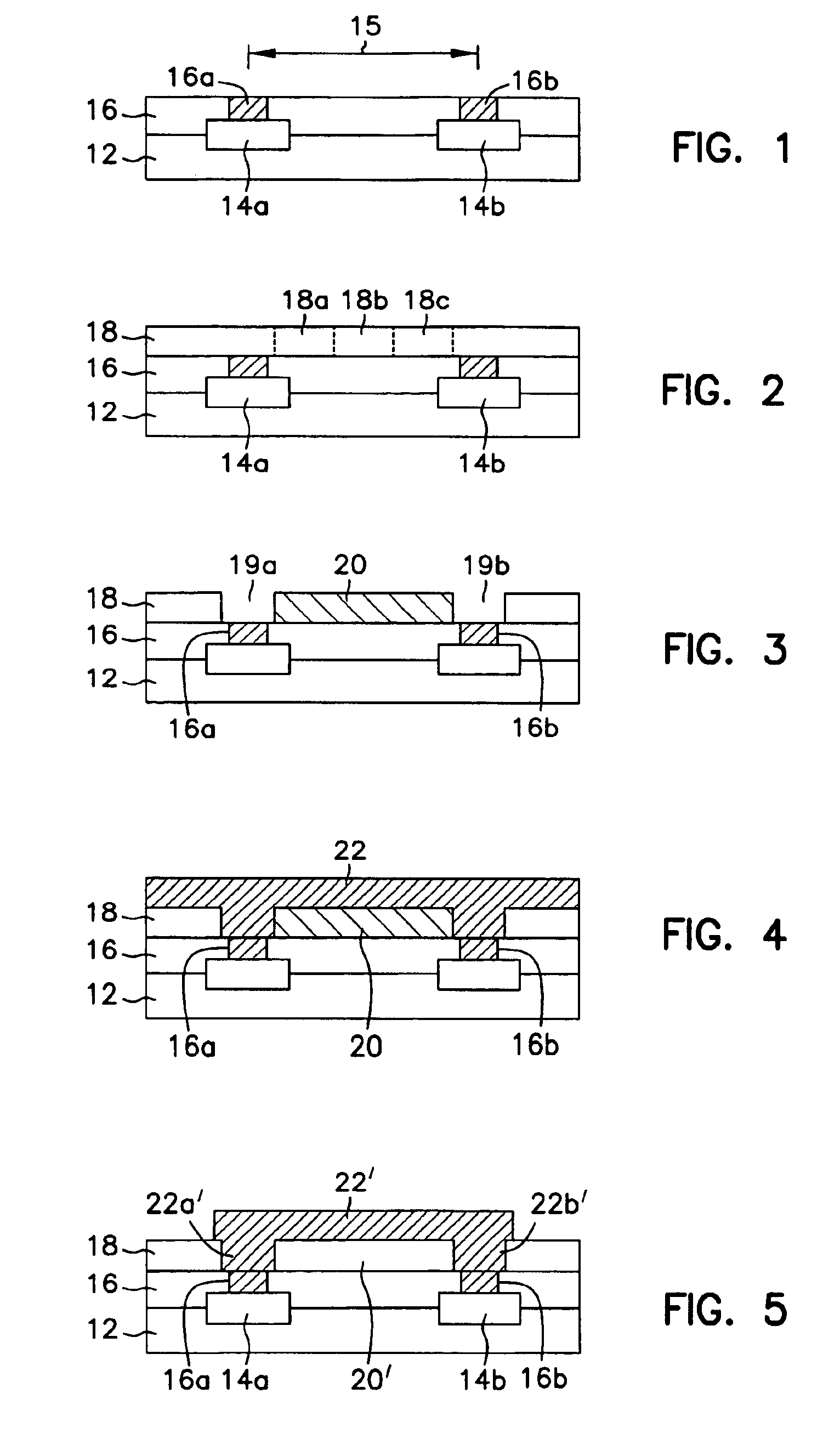
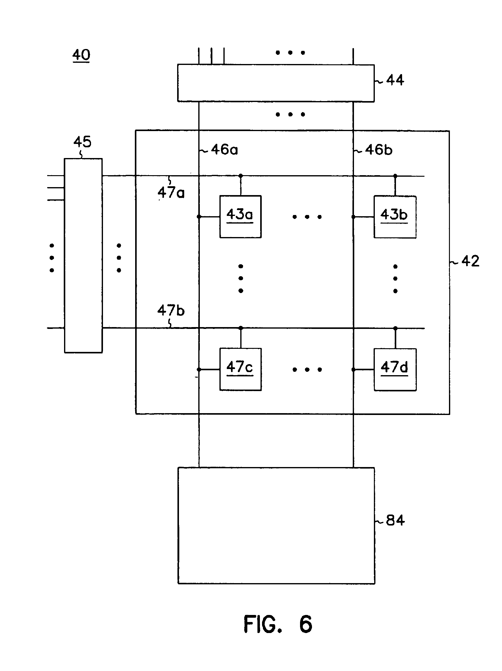
[0017]The following detailed description, which references and incorporates FIGS. 1-6, describes and illustrates one or more specific embodiments of the invention. These embodiments, offered not to limit but only to exemplify and teach the invention, are shown and described in sufficient detail to enable those skilled in the art to practice the invention. Thus, where appropriate to avoid obscuring the invention, the description may omit certain information known to those of skill in the art.

Definitions

[0018]The term “substrate,” as used herein, encompasses a semiconductor wafer as well as structures having one or more insulative, semi-insulative, conductive, or semiconductive layers and materials. Thus, for example, the term embraces silicon-on-insulator, silicon-on-sapphire, and other advanced structures.

[0019]The term “cavity” as used herein refers to a bounded, three-dimensional region having a dielectric constant different from areas outside the region. Thus, for example, the te...


PUM

PropertyMeasurementUnit
thicknessaaaaaaaaaa
thicknessaaaaaaaaaa
thicknessaaaaaaaaaa

Abstract

A typical air bridge is an aluminum conductor suspended across an air-filled cavity to connect two components of an integrated circuit, two transistors for example. The air-filled cavity has a low dielectric constant which reduces cross-talk between neighboring conductors and improves speed and efficiency of the integrated circuit. However, current air bridges must be kept short because typical aluminum conductors sag too much. Accordingly, one embodiment of the invention forms air-bridge conductors from an aluminum-beryllium alloy, which enhances stiffness and ultimately provides a 40-percent improvement in air-bridge lengths.

Description

[0001]This application is a Divisional of U.S. application Ser. No. 10 / 349,015, filed Jan. 21, 2003 now U.S. Pat. No. 6,717,191, which is a Continuation of U.S. application Ser. No. 09 / 119,355 filed Jul. 20, 1998, now U.S. Pat. No. 6,509,590, both of which are incorporated herein by reference.FIELD OF INVENTION[0002]The present invention concerns integrated circuits, particularly metals for forming air-bridge interconnects.BACKGROUND OF THE INVENTION[0003]Integrated circuits, the key components in thousands of electronic and computer products, are interconnected networks of electrical components fabricated on a common foundation, or substrate. Fabricators typically use various techniques, such as layering, doping, masking, and etching, to build thousands and even millions of microscopic resistors, transistors, and other electrical components on a silicon substrate, known as a wafer. The components are then “wired,” or interconnected, with aluminum wires to define a specific electric...

Claims


Application Information

Patent Timeline
Patent Type & Authority Patents(United States)
IPC IPC(8): C22C21/00H01L23/522H01L23/52H01L23/532
CPCC22C21/00H01L23/5221H01L23/53219H01L2924/0002H01L2924/00
Inventor FARRAR, PAUL A.
Owner CONVERSANT INTPROP MANAGEMENT INC
Why Eureka
Try Eureka