
Semiconductor integrated circuit apparatus

a technology of integrated circuit and semiconductors, applied in the direction of power consumption reduction, pulse technique, instruments, etc., can solve the problem that the application of a deep substrate bias does not have sufficient effect of reducing leakage current, and achieves the effects of enhancing the dibl effect, reducing drain voltage, and increasing the threshold voltage of the mos transistor

Inactive Publication Date: 2005-09-20
RENESAS ELECTRONICS CORP
View PDF16 Cites 15 Cited by
  • Summary
  • Abstract
  • Description
  • Claims
  • Application Information

AI Technical Summary

Benefits of technology

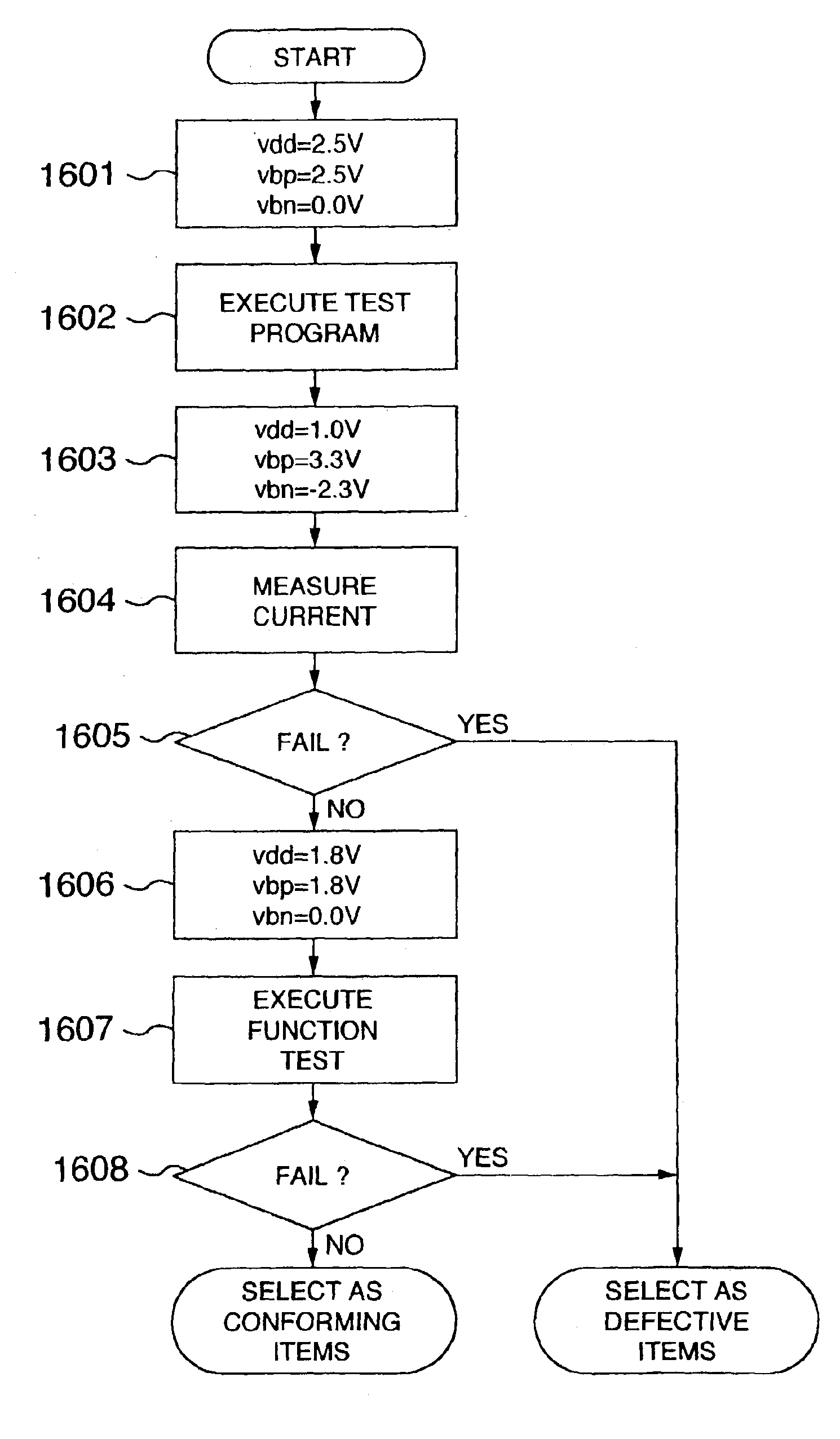
[0020]In a MOS transistor with a thin gate oxide having the gate voltage (Vgs) dependency of the drain current (Id) in off state as described above, the mere application of a deep substrate bias has no sufficient effect of reducing the leakage current. In FIG. 19, the curve D indicates the dependency characteristic in the case where a deep substrate bias is applied (Vbb=−2.3 V) and the drain voltage (Vds=1.0 V) is further reduced. By decreasing the power supply voltage in this way, a deep substrate bias can be applied to the well while limiting the voltage applied between the diffusion layer and the well of the MOS transistor to a small value (3.3 V in this case). Further, the following characteristics are obtained.
[0022](2) With the decrease in drain voltage, the drain induced barrier lowering (DIBL) effect increases the threshold voltage of the MOS transistor. In this case, the substrate bias is applied and therefore the DIBL effect is enhanced. (In FIG. 19, comparison between curves C and D shows that the leakage current is generally smaller, the lower the voltage Vds.)
[0023]Utilizing this dependency characteristic, the leakage current can be remarkably reduced when a transistor having a thin gate oxide is in off state. For realizing these substrate bias conditions with each MOS transistor when the chip is in standby mode, the power supply voltage of the transistor is required to be reduced below a normal operation level to further deepen the substrate bias to be applied.
[0025]on the other hand, JP-A-10-229165 laid open Aug. 25, 1998, discloses a method in which both the substrate bias voltage and the power supply voltage are controlled in standby mode, so that the change rate of the substrate bias voltage is reduced for changing the threshold voltage. This conventional method also fails to recognize that the means mentioned above, when included in a thin-film transistor, have the synergistic effect of reducing the leakage current, but discloses a technique of changing the change amount by controlling the substrate bias voltage and the power supply voltage instead of by changing the substrate bias voltage alone.

Problems solved by technology

In a MOS transistor with a thin gate oxide having the gate voltage (Vgs) dependency of the drain current (Id) in off state as described above, the mere application of a deep substrate bias has no sufficient effect of reducing the leakage current.
In this well-known method, however, each means involved is recognized to have an independent effect, but the fact fails to be recognized that these means have a synergistic effect of reducing the leakage current effectively in a thin-film transistor.
This conventional method also fails to recognize that the means mentioned above, when included in a thin-film transistor, have the synergistic effect of reducing the leakage current, but discloses a technique of changing the change amount by controlling the substrate bias voltage and the power supply voltage instead of by changing the substrate bias voltage alone.

Method used


Image

  • Semiconductor integrated circuit apparatus
  • Semiconductor integrated circuit apparatus
  • Semiconductor integrated circuit apparatus

Examples


Embodiment Construction

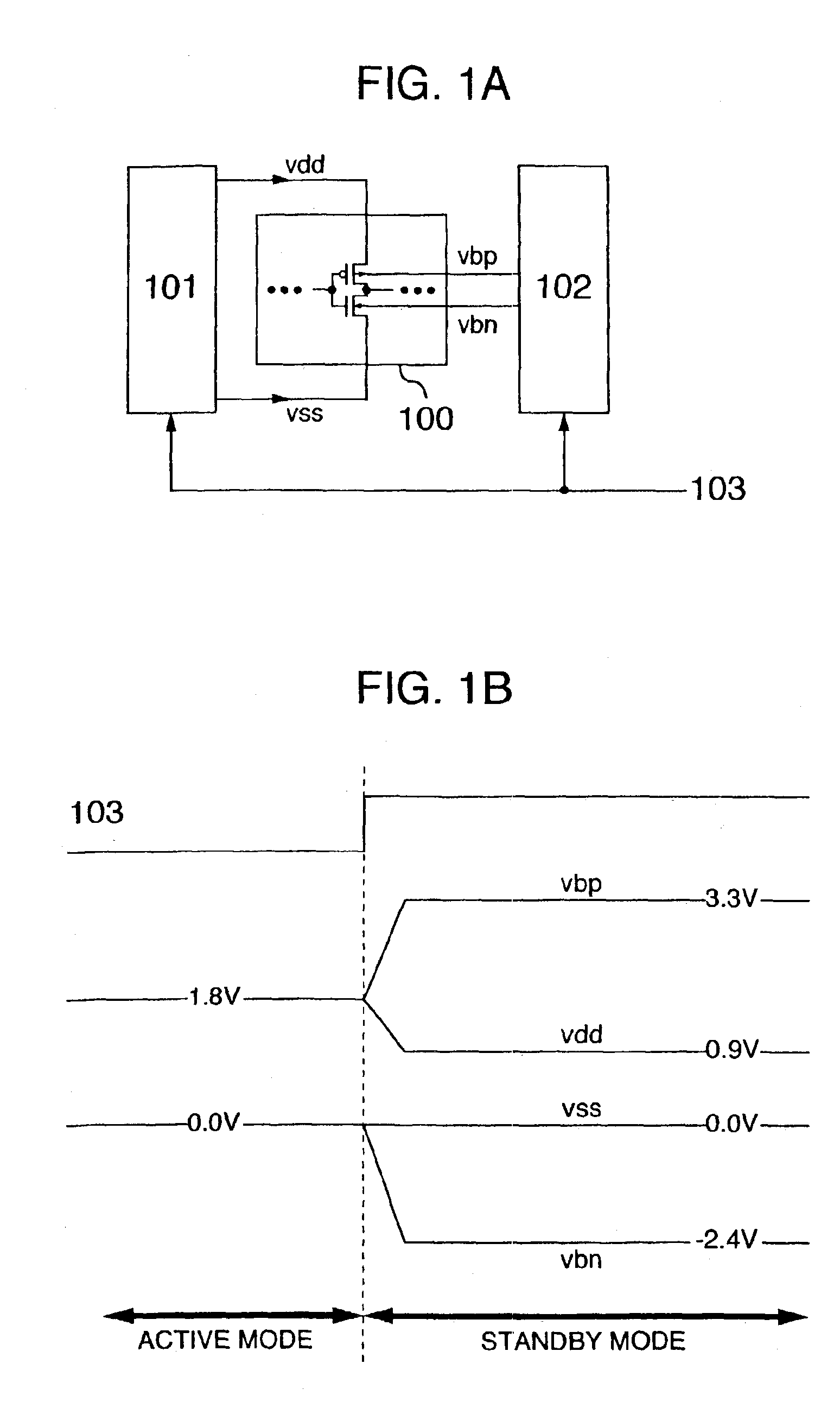
[0062]FIGS. 1A, 1B show a basic embodiment of the invention. Reference characters vdd designate a power supply voltage, vss a ground voltage, vbp a substrate bias voltage of a PMOS, vbn a substrate bias voltage of a NMOS, numeral 100 a circuit including a MOS transistor, numeral 101 a power supply voltage control circuit, numeral 102 a substrate bias control circuit, and numeral 103 a mode signal.

[0063]When the mode signal line 103 is “L”, a voltage of 1.8 V is applied as vdd and a voltage of 0 V as vss by the power supply voltage control circuit 101. Also, a voltage of 1.8 V is applied as vbp and a voltage of 0 V as vbn by the substrate bias control circuit 102. Thus, the circuit 100 enters an active mode and become capable of high-speed operation.

[0064]In the case where the mode signal 103 is “H”, on the other hand, a voltage of 0.9 V is applied as vdd and 0 V as vss by the power supply voltage control circuit 101. Also, a voltage of 3.3 V is applied as vbp and a voltage of −2.4 V...


PUM


Abstract

A semiconductor integrated circuit apparatus includes a first controlled circuit halving at least one MOS transistor and a substrate bias control unit for generating a substrate bias voltage of the MOS transistor, wherein when the substrate bias control unit is set in a first mode, a comparatively large current is allowed to flow between the source and drain of the MOS transistor, while when the substrate bias control unit is set in a second mode, the comparatively large current allowed to flow between the source and drain of the MOS transistor is controlled to a current of smaller value. The value of the substrate bias applied to the first controlled circuit is larger in the second mode than in the first mode for the substrate bias of the PMOS transistor, and smaller in the second mode than in the first mode for the substrate bias of the NMOS transistor. The power supply voltage applied to the first controlled circuit is controlled to a smaller value in the second mode than in the first mode.

Description

[0001]This is a continuation of application Ser. No. 10 / 024,039 filed 21 Dec. 2001, now U.S. Pat. No. 6,630,857 which is a division of application Ser. No. 09 / 390,962 filed 7 Sep. 1999, now U.S. Pat. No. 6,380,798, the content of which is incorporated herein by reference in its entirety.BACKGROUND OF THE INVENTION[0002]1. Field of the Invention[0003]The present invention relates to a semiconductor integrated circuit apparatus or more in particular to a semiconductor integrated circuit apparatus having a high speed and low power consumption at the same time.[0004]2. Description of the Related Art[0005]A CMOS circuit decreases in speed with a decrease in voltage. For the speed decrease to be complemented for, the threshold voltage of the MOS transistor (or the MIS transistor) is required to be reduced. The problem, however, is that the power consumption is increased by the subthreshold leakage current of the MOS transistor when the CMOS circuit is not in operation. A solution to this ...

Claims


Application Information

Patent Timeline
IPC IPC(8): H03K19/00G11C5/14
CPCH03K19/0016G02F1/1333B41F15/0881G02F1/133331
Inventor MIZUNO, HIROYUKIISHIBASHI, KOICHIRONARITA, SUSUMU
Owner RENESAS ELECTRONICS CORP
Learn More