Semiconductor device

a semiconductor and device technology, applied in semiconductor devices, instruments, electrical apparatus, etc., can solve the problems of affecting the performance of the device, the dielectric breakdown of the dielectric, and the inability to drive all pixels, so as to prevent age-based deterioration, high hot carrier resistance, and voltage resistance characteristics

Inactive Publication Date: 2005-09-27
SEMICON ENERGY LAB CO LTD
View PDF69 Cites 55 Cited by
  • Summary
  • Abstract
  • Description
  • Claims
  • Application Information

AI Technical Summary

Benefits of technology

[0011]The second impurity region is a low concentration impurity region that overlaps a gate electrode with a gate insulating film interposed therebetween, and has the effect of enhancing hot carrier resistance. On the other hand, the third impurity region is a low impurity region that does not overlap the gate electrode, and has the effect to prevent the off current from increasing.
[0019]An impurity concentration gradient can be formed in the inside of the second impurity region with this type of structure. The present invention is characterized by actively forming this type of such a concentration gradient, forming a TFT structure that enhances the electric field relaxation effect.
[0023]An NTFT with the above structure has high hot carrier resistance, and its voltage resistance characteristics (resistance to dielectric breakdown due to electric field concentration) are also good, so it is possible to prevent age-based deterioration in the on current (the current flow when the TFT is in an on state). This effect is due to the formation of the second impurity region.
[0024]In addition, it is possible to greatly reduce the off current by formation of the third impurity region. As outlined above, the formation of the third impurity region is a characteristic of the NTFT of the present invention.
[0025]The NTFT of the present invention has very high reliability. Thus it is possible to form a high reliability circuit when the NTFT is complementally combined with a PTFT to form a CMOS circuit, or used in a pixel region (pixel matrix circuit) of a liquid crystal display device or an electroluminescence display device. In other words, compared with a conventional NTFT, the drop in capability of a circuit due to deterioration of the NTFT can be prevented.

Problems solved by technology

A driver circuit that drives all of the pixels is therefore extremely complex, and furthermore is formed from a large number of TFTs.
If an abnormality occurs in the driver circuit, especially, this invites a fault called a line defect in which one column (or one row) of pixels turns off completely.
However, from a reliability point of view, TFTs that use polysilicon films still fall behind MOSFETs (transistors formed on a single crystal semiconductor substrate), etc., used in LSIs.

Method used


Image

  • Semiconductor device
  • Semiconductor device
  • Semiconductor device

Examples


embodiment mode 1

[Embodiment Mode 1]

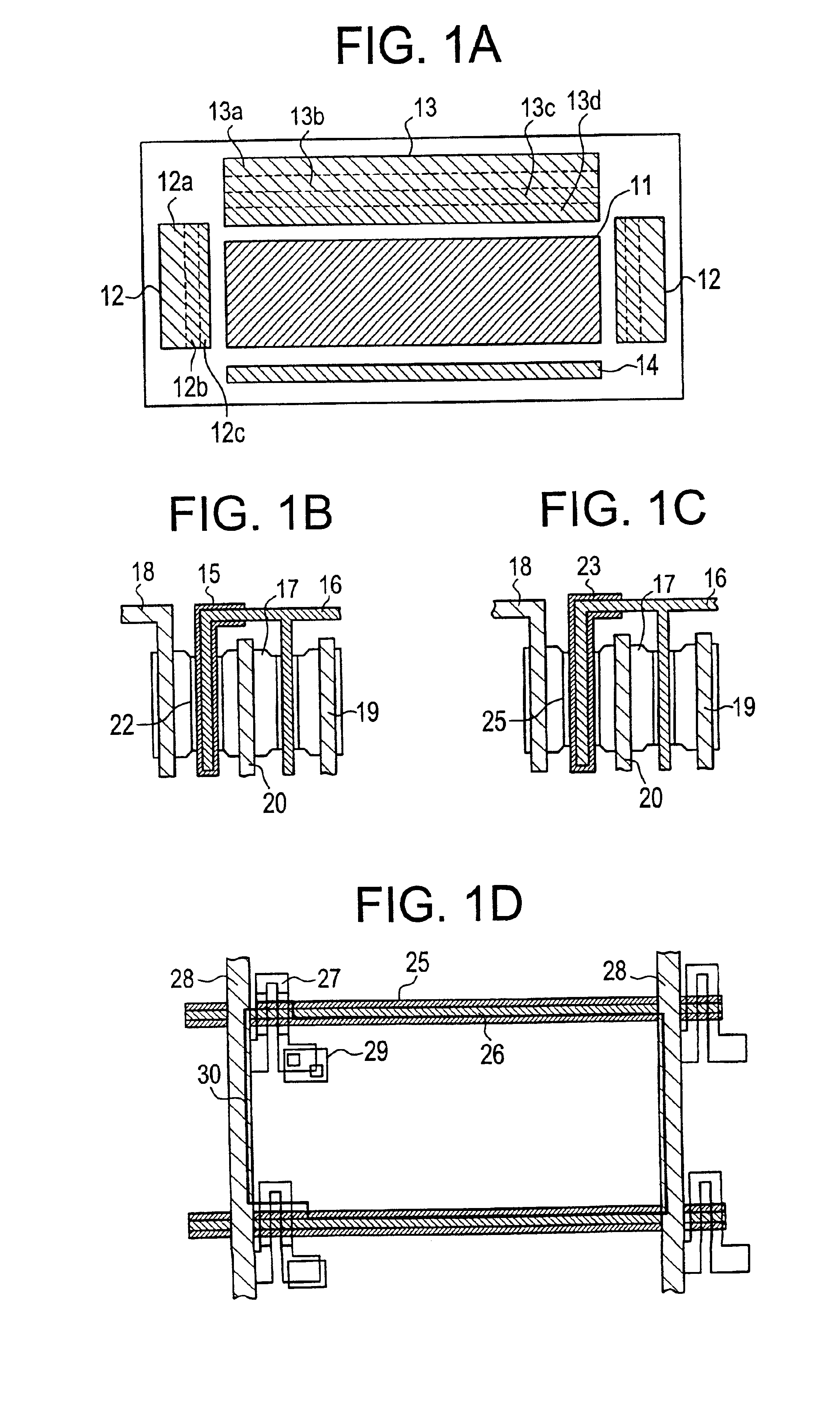
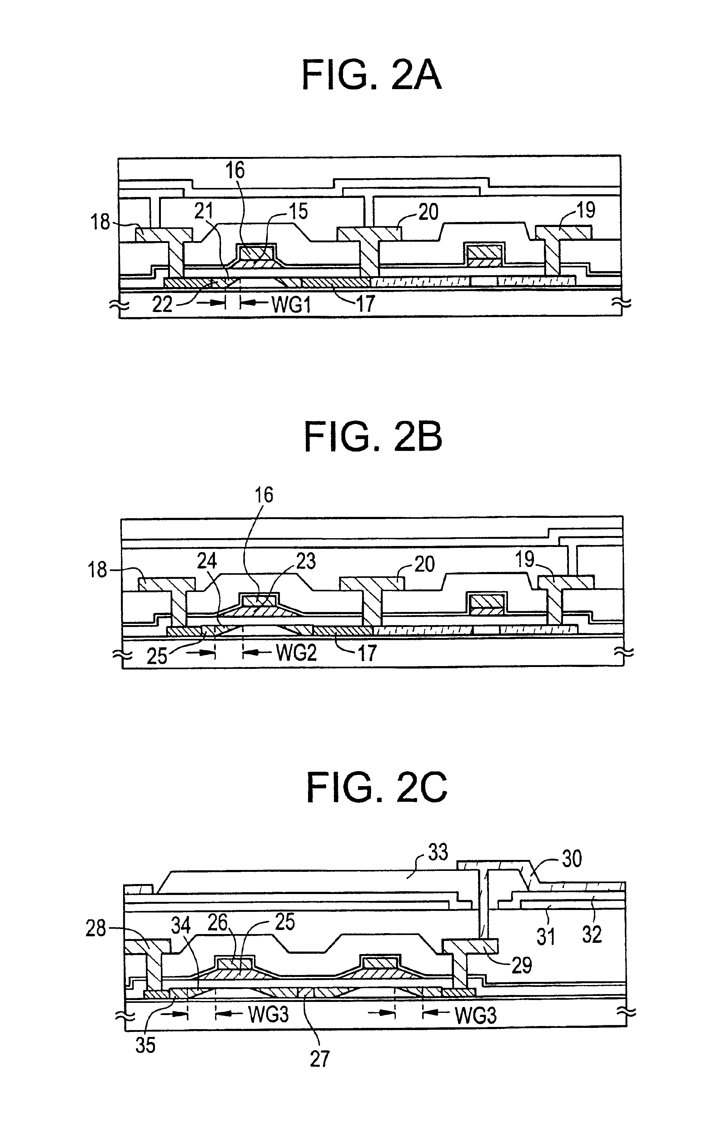
[0051]In Embodiment Mode 1, FIGS. 3A to 3D and FIGS. 4A to 4C are used to explain a manufacturing process of a TFT used in the present invention.

[0052]First, a base film 101 is formed over the entire surface of a substrate 100, and a semiconductor layer 102 with an island shape is formed on the base film 101. An insulating film 103 that becomes a gate insulating film is then formed over the entire surface area of the substrate 100, covering the semiconductor layer 102 (see FIG. 3A).

[0053]The following can be used as the substrate 100: a glass substrate; a quartz substrate; a crystalline glass substrate; a metallic substrate; a stainless steel substrate; and a resin substrate such as polyethylene terephthalate (PET).

[0054]The base film 101 is a film that prevents diffusion of mobile ions such as sodium ions, from the substrate 100 to the semiconductor layer 102, and increases adhesion of the semiconductor layer formed on the substrate 100. Either single layer or mu...

embodiment mode 2

[Embodiment Mode 2]

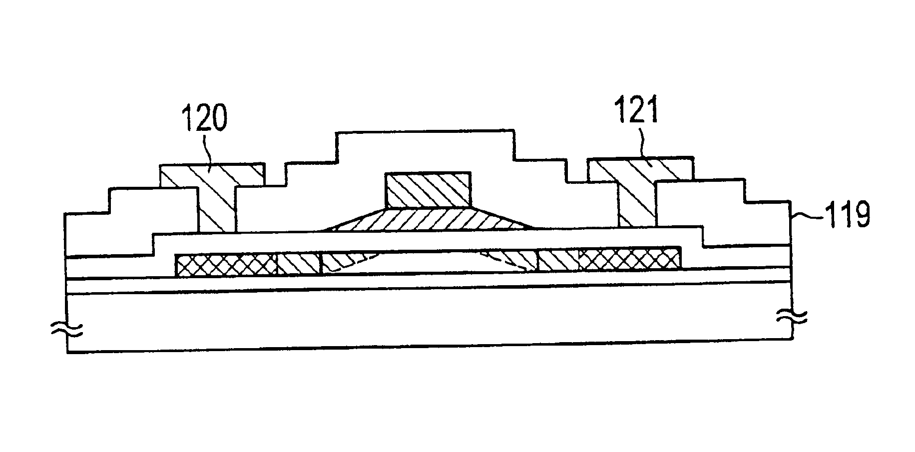
[0098]Embodiment Mode 2 is an example in which the gate electrode (gate wiring) structure is different than in Embodiment Mode 1. Specifically, the gate electrode has a laminated structure of two gate electrodes with different widths in Embodiment Mode 1, but in Embodiment Mode 2 the upper second gate electrode is omitted, and the gate electrode is formed from only a first gate electrode, which has a tapered portion.

[0099]Embodiment Mode 2 is shown in FIG. 7. Note that structurally it is nearly identical to Embodiment Mode 1, so that only the different points are labeled with a reference numeral and explained.

[0100]In FIG. 7 the point of difference from the structure shown in FIG. 4C is that a gate electrode 130 is formed from a single layer film. Therefore the explanation of Embodiment Mode 1 applies to all other portions.

[0101]A material that can easily be taper etched is desirable for the conductive film that becomes the gate electrode 130. Regarding the thin f...

embodiment 1

[Embodiment 1]

[0111]Embodiment 1 shows an example in which the NTFT explained in the embodiment modes is used to fabricate an active matrix type liquid crystal display device (AM-LCD).

[0112]FIG. 8 is a schematic structural view of the AM-LCD of Embodiment 1. The AM-LCD has a structure with a liquid crystal sandwiched between an active matrix substrate 200 and an opposing substrate 206. The active matrix substrate 200 has a pixel region 201, a gate driver circuit 202 that drives the pixel region 201, and a source driver circuit 203 thereon. These driver circuits are connected to the pixel region 201 by source wirings and drain wirings, respectively.

[0113]In addition, a signal processing circuit 204 is formed on the substrate in order to process the video signals transmitted to the source driver circuit 203. A D / A converter circuit, a signal division circuit, a v correction circuit, etc., can be given as examples of the signal processing circuit. Then, an external terminal is formed i...


PUM

PropertyMeasurementUnit
taper angleaaaaaaaaaa

Abstract

In order to realize a higher reliability TFT and a high reliability semiconductor device, an NTFT of the present invention has a channel forming region, n-type first, second, and third impurity regions in a semiconductor layer. The second impurity region is a low concentration impurity region that overlaps a tapered potion of a gate electrode with a gate insulating film interposed therebetween, and the impurity concentration of the second impurity region increases gradually from the channel forming region to the first impurity region. And, the third impurity region is a low concentration impurity region that does not overlap the gate electrode.Moreover, a plurality of NTFTs on the same substrate should have different second impurity region lengths, respectively, according to difference of the operating voltages. That is, when the operating voltage of the second TFT is higher than the operating voltage of the first TFT, the length of the second impurity region is longer on the second TFT than on the first TFT.

Description

BACKGROUND OF THE INVENTION[0001]1. Field of the Invention[0002]The present invention relates to a thin film transistor (hereinafter referred to as TFT) and to a semiconductor device having a circuit structured with a thin film transistor. The present invention relates to such semiconductor devices as electro-optical devices, typically active matrix liquid crystal display devices (hereinafter referred to as AM-LCDs), and semiconductor circuits including processors, etc. The present invention also relates to electronic equipment loaded with the electro-optical devices or semiconductor circuits. Note that throughout this specification semiconductor device indicates general devices that acquire their function through the use of semiconductor characteristics, and that electro-optical devices, semiconductor circuits, and electronic equipment are semiconductor devices.[0003]2. Description of the Related Art[0004]Active matrix type liquid crystal display devices composed of TFT circuits th...

Claims


Application Information

Patent Timeline
Patent Type & Authority Patents(United States)
IPC IPC(8): H01L21/70H01L27/12H01L21/84G02F1/13G02F1/1362H01L21/77
CPCH01L27/1214H01L29/42384G02F1/13454H01L2029/7863
Inventor YAMAZAKI, SHUNPEI
Owner SEMICON ENERGY LAB CO LTD
Why Eureka
Try Eureka