Magnetic memory device capable of passing bidirectional currents through the bit lines

a memory device and bidirectional current technology, applied in nanoinformatics, instruments, substrates/intermediate layers, etc., can solve the problems of long time and disadvantageous power consumption in writing, and achieve the effect of reducing parasitic capacitance of mosfet, reducing manufacturing cost, and high operation speed of mos

Inactive Publication Date: 2005-09-27
RENESAS ELECTRONICS CORP
View PDF15 Cites 72 Cited by
  • Summary
  • Abstract
  • Description
  • Claims
  • Application Information

AI Technical Summary

Benefits of technology

[0141]Since the magnetic substrate of the twenty-fourth aspect of the present invention at least has the multilayer film provided entirely on a main surface thereof to make up at least one magnetic tunnel junction, in manufacturing the magnetic memory device comprising the memory cells having at least one magnetic tunnel junction, the manufacturing process can be omitted and the manufacturing cost can be cut as compared with a case where a simple semiconductor substrate is prepared and the multilayer film is formed on a main surface thereof.
[0142]In the twenty-fifth aspect of the present invention, it is possible to obtain a magnetic substrate suitable to manufacture the magnetic memory device comprising a memory cell having a single magnetic tunnel junction.
[0143]In the twenty-sixth aspect

Problems solved by technology

For this reason, the power consumption in writing disadvantageously becomes large.
Further, the background-art MRAM cell array has a problem that it ta

Method used


Image

  • Magnetic memory device capable of passing bidirectional currents through the bit lines
  • Magnetic memory device capable of passing bidirectional currents through the bit lines
  • Magnetic memory device capable of passing bidirectional currents through the bit lines

Examples


Embodiment Construction

[0200]

[0201]

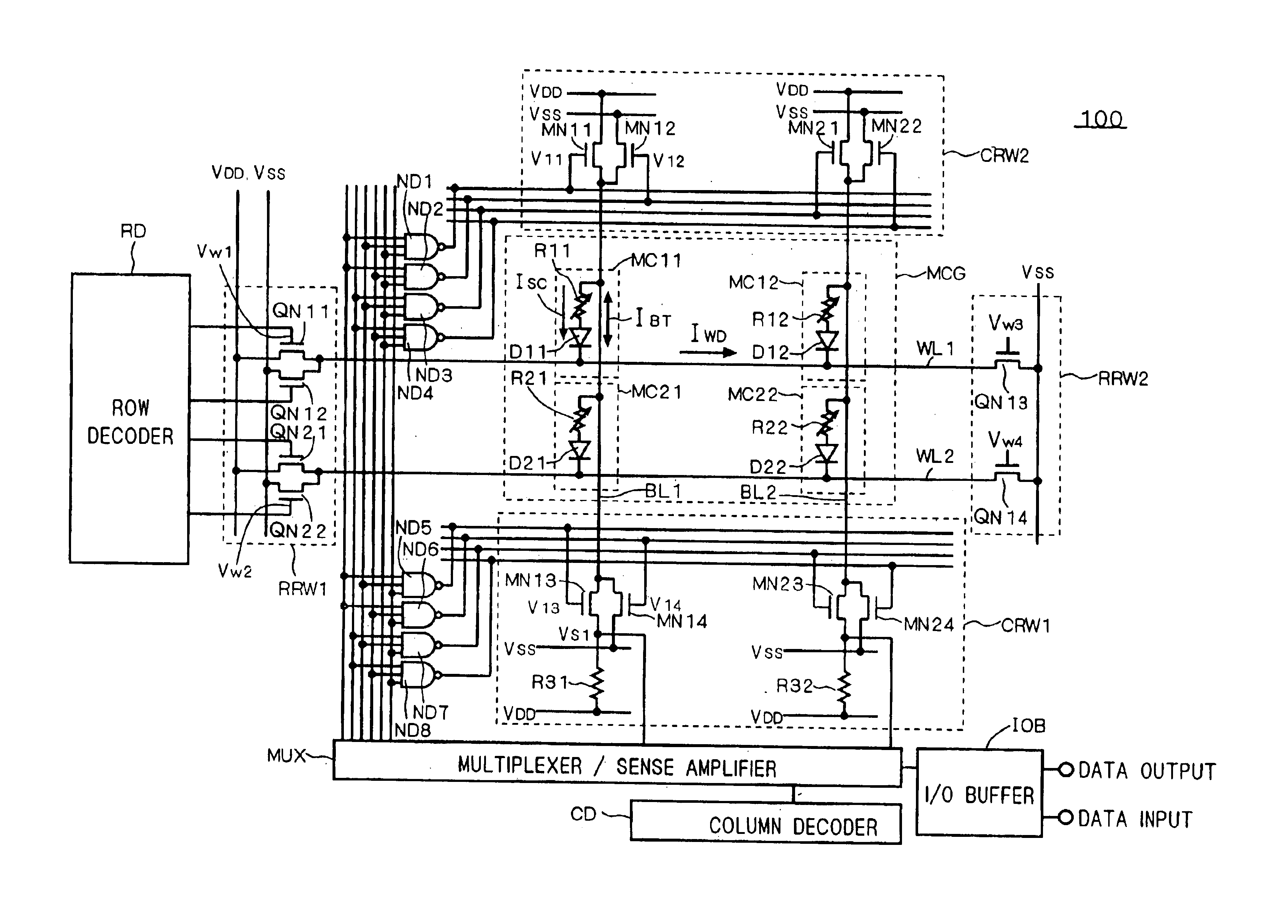
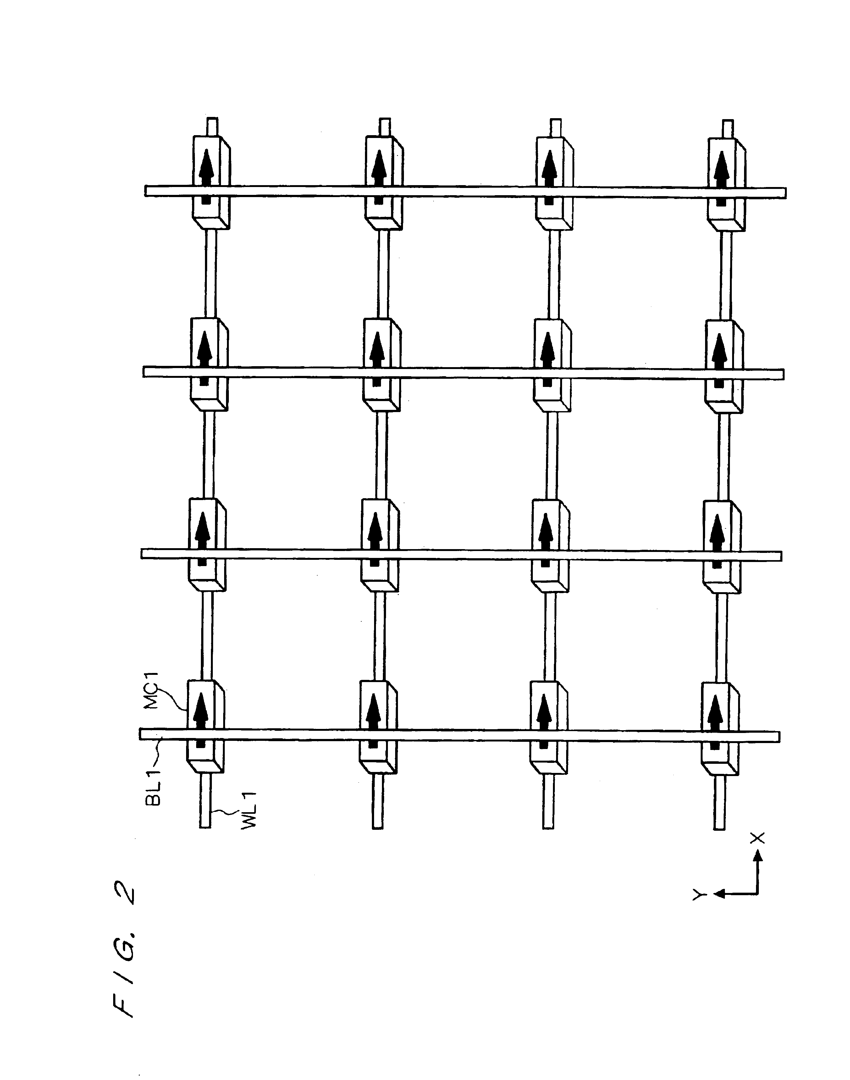
[0202]An MRAM in accordance with the first preferred embodiment of the present invention is characteristically provided so that an easy axis of a soft ferromagnetic layer which is a constituent element of an MRAM cell may not be parallel to bit lines or word lines, and more specifically, may have an angle of 40 to 50 degrees with respect to the bit lines and the word lines.

[0203]

[0204]

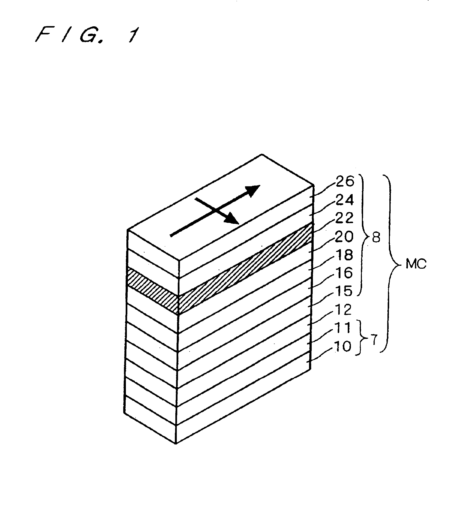
[0205]First, a typical structure of an MRAM cell will be discussed, referring to FIG. 1. An MRAM cell MC shown in FIG. 1 has the pn-junction diode 7 constituted of the n+ silicon layer 10 and the p+ silicon layer 11 which are layered.

[0206]The tungsten stud 12 is formed above the pn-junction diode 7, and the pn-junction diode 7 is electrically connected to the magnetic tunnel junction (MTJ) 8 through the tungsten stud 12.

[0207]MTJ 8 has a layered structure consisting of the template layer 15 (having a film thickness of 10 nm) made of platinum (Pt), the initial ferromagnetic layer 16 (having...


PUM


Abstract

A plurality of word lines (WL1) are provided in parallel to one another and a plurality of bit lines (BL1) are provided in parallel to one another, intersecting the word lines (WL1) thereabove. MRAM cells (MC2) are formed at intersections of the word lines and the bit lines therebetween. MRAM cells (MC3) are provided so that an easy axis indicated by the arrow has an angle of 45 degrees with respect to the bit lines and the word lines. Thus, an MRAM capable of cutting the power consumption in writing is achieved and further an MRAM capable of reducing the time required for erasing and writing operations is achieved.

Description

[0001]This application is a divisional of application Ser. No. 10 / 424,086 filed Apr. 28, 2003, now U.S. Pat. No. 6,741,495 which is a divisional of application Ser. No. 09 / 989,155, filed Nov. 21, 2001, now U.S. Pat. No. 6,567,299BACKGROUND OF THE INVENTION[0002]1. Field of the Invention[0003]The present invention relates to a magnetic memory device, and more particularly to a magnetic memory device having a nonvolatile memory cell array which uses a magnetic tunnel junction as each memory cell.[0004]2. Description of the Background Art[0005]<Tunnel Magnetic Resistance Effect>[0006]A structure in which an insulative material is sandwiched between two ferromagnetic materials is termed “magnetic tunnel junction (MTJ)”.[0007]FIG. 67 shows a concept of an MTJ. In FIG. 67, an insulating layer TB is provided, being sandwiched between ferromagnetic layers FM21 and FM22 and a voltage is applied to the ferromagnetic layers FM21 and FM22.[0008]In this structure, when a current tunneling ...

Claims


Application Information

Patent Timeline
IPC IPC(8): G11C11/15G11C11/16G11C11/02G11C11/14H01F10/08H01F10/32H01L21/8246H01L27/105H01L43/08
CPCB82Y10/00G11C11/15G11C11/16H01L2924/1305H01L2924/13091H01L2924/01068H01L2924/01021H01L2924/01019H01L2224/16H01L2224/48091H01L2224/48247H01L2924/01025H01L2924/01039H01L2924/01057H01L2924/01077H01L2924/01078H01L2924/15311H01L2924/19041H01L2924/30107H01L2924/3025H01L2924/00014H01L2924/00H01L2924/181G11C11/1675H01L2924/00012
Inventor KUNIKIYO, TATSUYAEIKYU, KATSUMI
Owner RENESAS ELECTRONICS CORP
Why Eureka
Try Eureka