

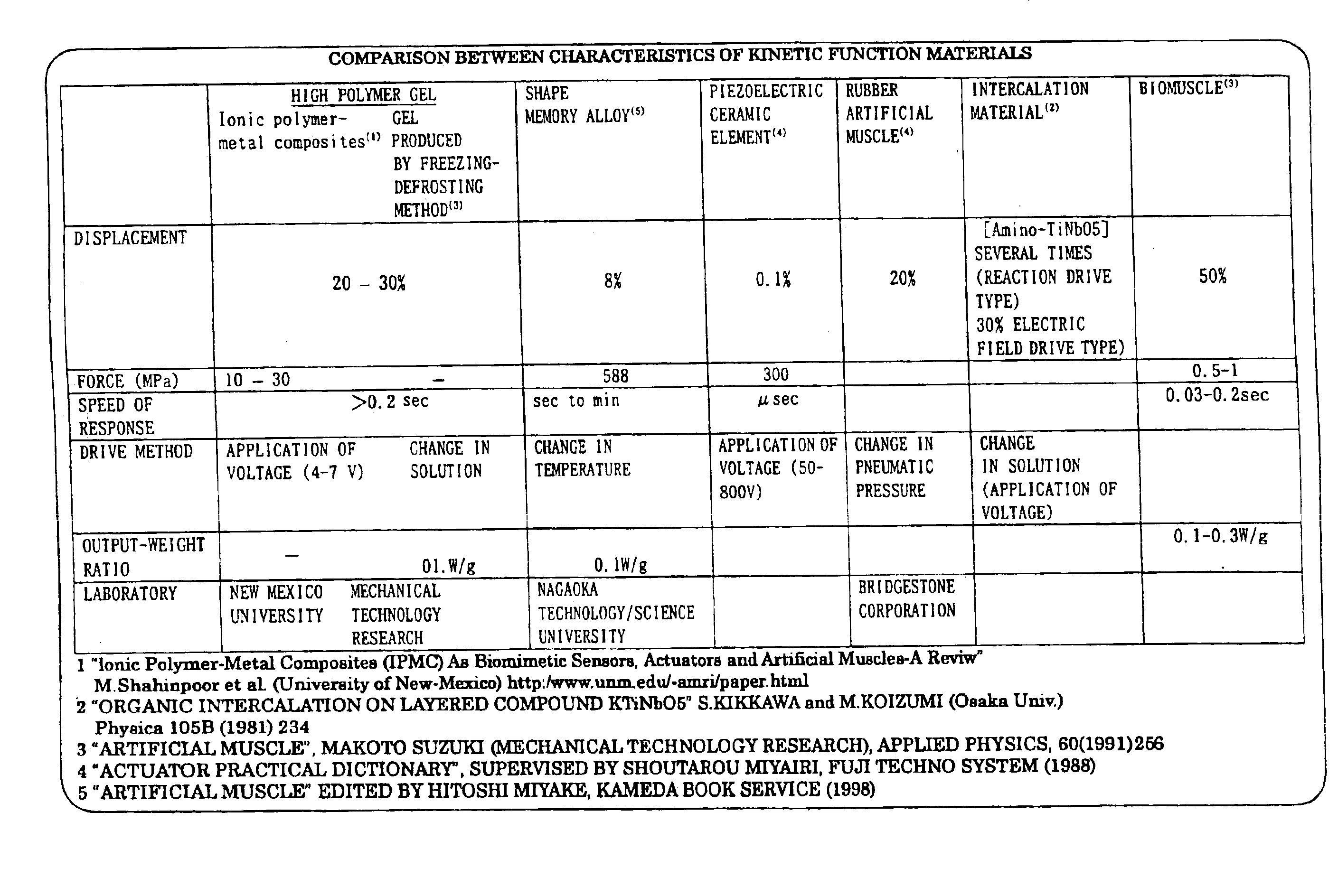
Functional material and functional device
a functional material and material technology, applied in the field of functional materials and functional devices, can solve the problems of non-linear material not being controlled from external, inability to select the wavelength of laser light from external after the production of optical devices, and inability to select the wavelength of laser light from external after the production of laser diodes, so as to reduce the noise of environmental light and easily change the refractive index of foreign matter
- Summary
- Abstract
- Description
- Claims
- Application Information
AI Technical Summary
Benefits of technology
Problems solved by technology
Method used
Image

Examples
embodiment 1
[Embodiment 1]
[0158]An optical functional device according to a first embodiment of the present invention will be described with reference to FIGS. 3 to 10.
[0159]A unit cycle of a periodic structure of an optical functional device is, as described above, selected at a value on the order of a wavelength of a transverse wave such as an electromagnetic wave or a longitudinal wave such as a sound wave to be modulated. In this embodiment, description will be made by example of a one-dimensional periodic structure configured to be matched to a visible light wavelength range as one of wavelength ranges of electromagnetic transverse waves. Such description can be of course extended to a two-dimensional or three-dimensional periodic structure.
[0160]FIG. 3 shows a one-dimensional periodic structure composed of multi-layer film in which two kinds of materials 1 and 2 are alternately, periodically stacked to each other. The material 1 is represented by SiO2 which has a refractive index approxim...
embodiment 2
[Embodiment 2]
[0170]An optical functional device according to a second embodiment will be described with reference to FIGS. 11 to 14.
[0171]Unlike the first embodiment in which the thickness of the M layer inserted as the foreign matter later in the one-dimensional periodic structure is changed, according to the second embodiment, the thickness of a foreign matter layer is kept constant and the dielectric constant, that is, the refractive index of the foreign matter layer is changed.
[0172]With a foreign matter layer (thickness: specified at 55 nm) is inserted taken as a sample, the wavelength shift of a mobile peak MP depending on a change in refractive index of the foreign matter layer from 1 to 5 is calculated. The result is shown in FIG. 11. As is apparent from this figure, a spike-like MP appears in a stop band, which shifts on the long-wavelength side with an increase in refractive index “n”. Similarly, with a foreign matter layer (thickness: specified at 220 nm) is inserted tak...
embodiment 3
[Embodiment 3]
[0178]An artificially modulated light skin according to a third embodiment of the present invention will be described with reference to FIG. 15. The artificially modulated light skin in this embodiment is based on the basic principle of the first or second embodiment.
[0179]Referring to FIG. 15, in the artificially modulated light skin in this embodiment, a one-dimensional photonics periodic structure similar to that described in the second embodiment, which is composed of a periodic multi-layer film 12 having a one-dimensional periodic structure in which a foreign matter thin film 13 is inserted, is formed on a base 11 functioning as an artificial skin. Conductive electrode films 14 and 15 are formed at interfaces between the periodic multi-layer film 12 and the foreign mater thin film 13. The foreign matter thin film 13 is made from a material whose kinetic function, or dielectric constant or refractive index is changeable when an electric field is applied thereto fro...
PUM
| Property | Measurement | Unit |
|---|---|---|
| speed | aaaaa | aaaaa |
| speed | aaaaa | aaaaa |
| frequency | aaaaa | aaaaa |
Abstract
Description
Claims
Application Information