Ceramic heater system and substrate processing apparatus having the same installed therein

a heater system and substrate technology, applied in the direction of ohmic resistance heating, electric heating, coatings, etc., can solve the problems of long cooling time, less heating performance of heaters, etc., to achieve high cooling efficiency and maintain high heating performance on the heating surfa

Inactive Publication Date: 2005-10-04
TOKYO ELECTRON LTD
View PDF34 Cites 426 Cited by
  • Summary
  • Abstract
  • Description
  • Claims
  • Application Information

AI Technical Summary

Benefits of technology

[0013]Accordingly, it is an object of the present invention to provide a ceramic heater system which has a high cooling efficiency while keeping t

Problems solved by technology

The cooling requires a long time.
This technique has been developed to mainly ensure uniform heating and does not provide a sufficient cooling performance.
Therefore, the more the heating efficiency is improved, the less the perfo

Method used


Image

  • Ceramic heater system and substrate processing apparatus having the same installed therein
  • Ceramic heater system and substrate processing apparatus having the same installed therein
  • Ceramic heater system and substrate processing apparatus having the same installed therein

Examples


first embodiment

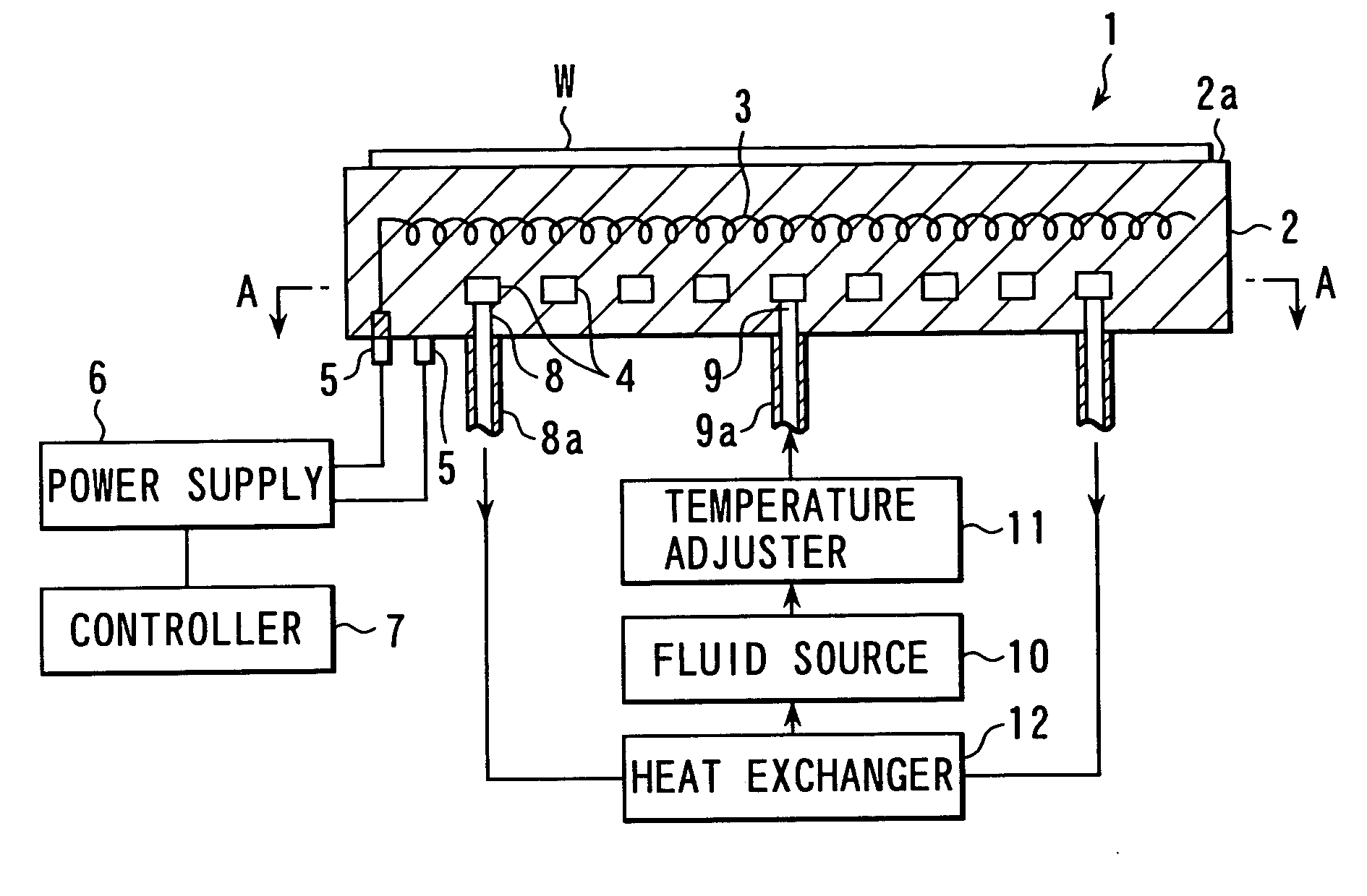
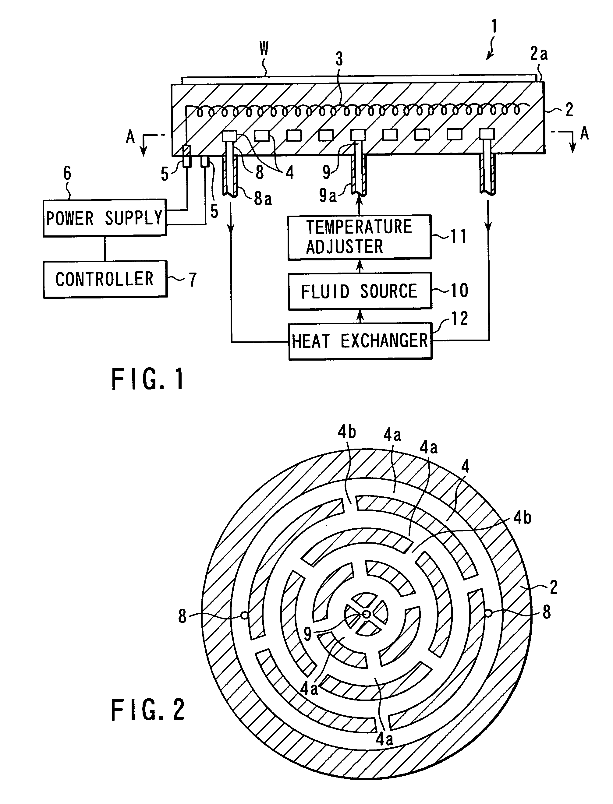
[0034]FIG. 1 is a vertical cross-sectional view exemplarily illustrating a ceramic heater system for processing a semiconductor wafer according to the invention. FIG. 2 is a horizontal cross-sectional view taken along the line A—A in FIG. 1.

[0035]A ceramic heater system 1 has a disk-shaped heater base 2 of ceramics and a heating resistive element (heater) 3 buried in the heater base 2 in a coil form. A fluid passage 4 is provided in the heater base 2 below the heater 3.

[0036]Any dense ceramics may be used for the heater base 2. Preferable ceramics for the heater base 2 include nitride ceramics, such as silicon nitride (Si3N4), aluminum nitride (AlN) and silicon aluminum oxy nitride (SiAlON), and aluminum oxide (Al2O3). The top surface of the heater base 2 serves as a mounting surface 2a for a semiconductor wafer W.

[0037]The heater 3, which is a heat resistor, is buried in the heater base 2 in a predetermined pattern (e.g., a spiral form) with its both end portions connected to termi...

second embodiment

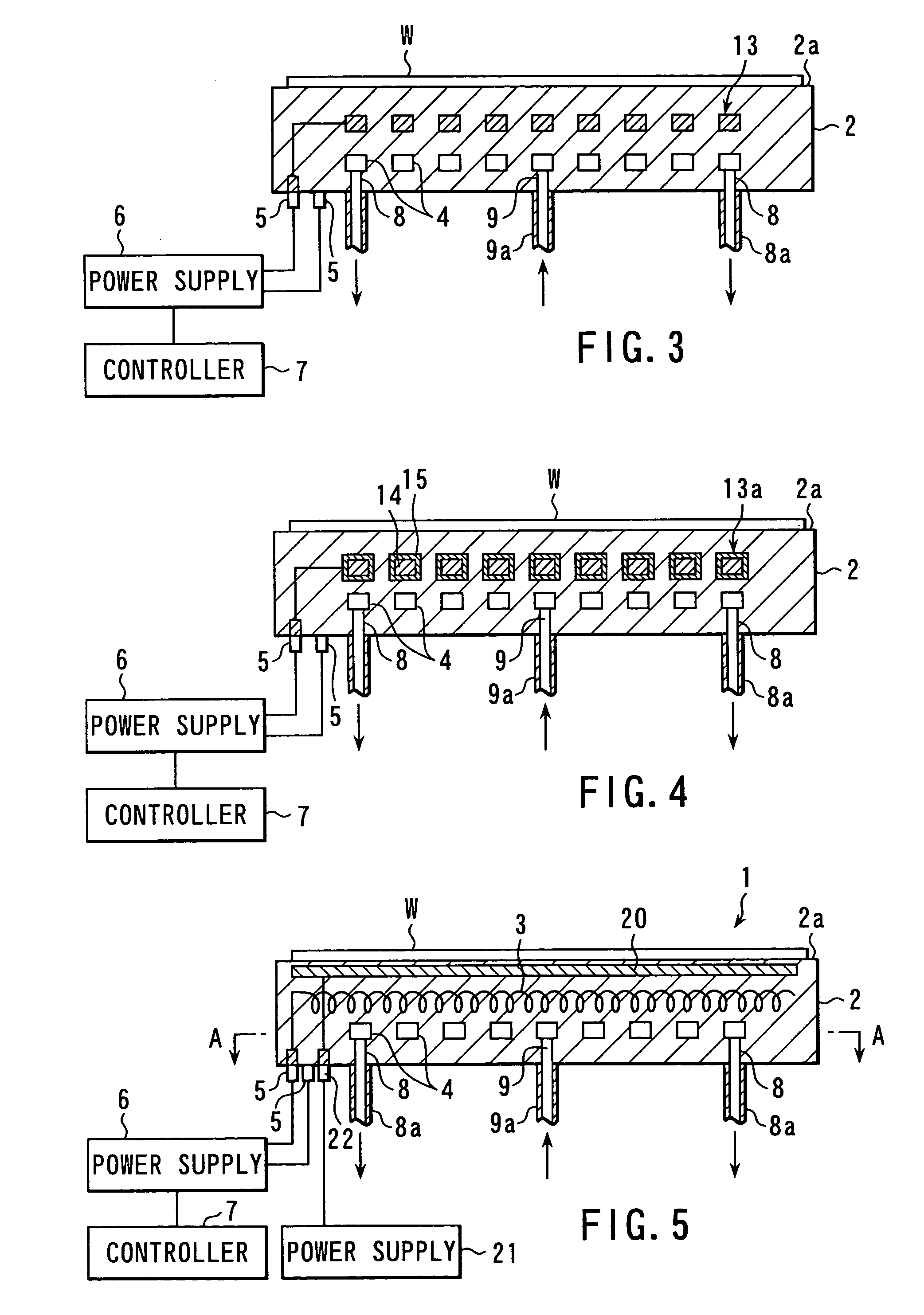
[0046]In the ceramic heater system of the second embodiment, a heater 13 buried in the heater base 2 is formed of graphite or glassy carbon and is arranged in a predetermined pattern (e.g., a spiral form).

[0047]In the ceramic heater system, the coefficients of thermal expansion of graphite and glassy carbon, materials for the heater 13, are respectively 2 to 3×10⁻⁶ / K and 1.5×10⁻⁶ / K to 2.5×10⁻⁶ / K, which are relatively close to the coefficient of thermal expansion of AlN of 4.6×10⁻⁶ / K, so that the heater base 2 can be used without being damaged even if the temperature is raised fast or dropped fast.

[0048]As a modification of the second embodiment shown in FIG. 4, a heater 13a having a core 14 of graphite or glassy carbon coated with a glassy BN layer 15 may be used. In this case, the glassy BN has a function of protecting the core 14 of graphite or glassy carbon and a buffer capability, thus ensuring faster temperature raising and faster temperature drop.

[0049]A ceramic heater system ...

third embodiment

[0053]In the case where a plasma treatment is carried out by using the ceramic heater of each of the above-described embodiments, a plasma-producing electrode 23 is buried in the heater base 2 as in a modification of the third embodiment shown in FIG. 6. Plasma can be produced by grounding the electrode 23 and applying high-frequency power to the opposing electrode in the vacuum atmosphere. A DC voltage is applied to the electrode provided below the counter electrode. The DC voltage functions as a bias introducing ions and flaxes into the substrate. The etching rate and the deposition rate are thereby enhanced.

[0054]High-frequency power may be applied to the electrode 23. Instead of ground the electrode 23, a DC voltage may be applied to the electrode 23 so that the electrode 23 also serves as an electrode for the electrostatic chuck.

[0055]A ceramic heater system according to the fourth embodiment of the invention will now be described with reference to FIG. 7 which shows the cross ...


PUM

PropertyMeasurementUnit
Temperatureaaaaaaaaaa
Electric potential / voltageaaaaaaaaaa
Metallic bondaaaaaaaaaa

Abstract

A ceramic heater system has a ceramic heater base having a substrate-mounting surface formed on the top surface thereof and a heater, buried in the heater base, for heating a substrate. A fluid passage is formed buried in the heater base below where the heater is buried. The heater base is cooled as a fluid whose temperature is lower than the temperature of the heater base is let flow in the fluid passage. A substrate processing apparatus has the ceramic heater system installed in a process chamber whose vacuum state can be maintained, a gas supply mechanism for feeding a gas into the process chamber, and a power supply. The substrate processing apparatus performs a heat treatment, etching and film deposition on a substrate placed in the process chamber.

Description

CROSS-REFERENCE TO RELATED APPLICATIONS[0001]This application is based upon and claims the benefit of priority from the prior Japanese Patent Application No. 11-341916, filed Dec. 1, 1999, the entire contents of which are incorporated herein by reference.BACKGROUND OF THE INVENTION[0002]The present invention relates to ceramic heater system which heats a substrate in treatments, such as CVD (Chemical Vapor Deposition) and plasma etching, and to a substrate processing apparatus having this heater system installed therein.[0003]The general fabrication of semiconductor devices includes a step of performing a vacuum treatment, such as CVD or plasma etching, on a semiconductor wafer to be processed. In such a treatment, a heat treatment for heating a semiconductor wafer to a predetermined temperature is carried out. To execute such a heat treatment, a heater is buried in a substrate support member. A typical conventional heater of this type is a stainless heater.[0004]Ceramic heaters tha...

Claims


Application Information

Patent Timeline
IPC IPC(8): C23C16/00C23F1/00H01L21/02H01L21/205H01L21/306H05B3/20H01L21/302C23C16/458H01L21/00H01L21/3065
CPCC23C16/4586H01L21/67109
Inventor NARUSHIMA, MASAKI
Owner TOKYO ELECTRON LTD
Why Eureka
Try Eureka