Interface circuit coupling semiconductor test apparatus with tested semiconductor device

a test apparatus and interface circuit technology, applied in the direction of logic circuit coupling/interface arrangement, measurement devices, instruments, etc., can solve the problems of preventing an accurate test, deteriorating the waveform quality of the output signal, and the low power supply voltage type of lsi cannot be tested with the tester, so as to reduce the test cost and improve the test accuracy

Inactive Publication Date: 2005-10-11
RENESAS ELECTRONICS CORP
View PDF11 Cites 24 Cited by
  • Summary
  • Abstract
  • Description
  • Claims
  • Application Information

AI Technical Summary

Benefits of technology

[0009]A main object of the present invention is therefore to provide an interface circuit where a test cost can be reduced and test accuracy can be improved.
[0010]An interface circuit includes a plurality of buffer circuits provided respectively corresponding to a plurality of tested semiconductor devices and having their input nodes connected to each other, each transmitting an output signal of the semiconductor test apparatus to a corresponding tested semiconductor device. Therefore the number of devices that can be measured by the semiconductor test apparatus at a time can be increased by multiple times and the test cost can be reduced. Furthermore, since each of a plurality of distributing paths is provided with a buffer, the same current and a signal of the same waveform can be applied to a plurality of tested semiconductor devices and a test can be performed accurately.
[0011]Another interface circuit in accordance with the present invention includes: a first buffer circuit having its input node receiving an output signal of a semiconductor test apparatus; a load circuit suppressing a reflection of a signal output from a first tested semiconductor device; a first switching circuit having a first switch terminal receiving an output signal of the first buffer circuit, a second switch terminal connected to the first tested semiconductor device and a third switch terminal connected to the load circuit, being rendered conductive between the first and second switch terminals at a first mode in which an output signal of the semiconductor test apparatus is applied to the first tested semiconductor device, and being rendered conductive between the second and third switch terminals at a second mode in which an output signal of the first tested semiconductor device is applied to the semiconductor test apparatus; and a second buffer circuit having its input node connected to the second switch terminal and transmitting an output signal of the first tested semiconductor device to the semiconductor test apparatus at the second mode. Therefore with a shortened distance between the interface circuit and the tested semiconductor device, a length of a portion where a mismatch is caused between the semiconductor test apparatus and the tested semiconductor device can be reduced. As a result, the effect of the signal reflection can be reduced and a test can be performed accurately. Furthermore, the life of the semiconductor test apparatus can be prolonged and the test cost can be reduced.

Problems solved by technology

With only parallel connection of an output pin of a tester with a plurality of LSIs, a mismatch of an output impedance of the tester may be caused to deteriorate a waveform quality of the output signal or an output current of the tester may not be distributed evenly to a plurality of LSIs, thereby preventing an accurate test.
However, the low power supply voltage type of LSI cannot be tested with the tester that has tested the high power supply voltage type of LSI, because the resolution of the output voltage is coarse.
Therefore, a tester having a high voltage-accuracy is separately needed, thereby increasing the test cost.
Therefore, because of a mismatch between an impedance of an external pin of a commercially available tester (mainly 50 Ω) and an output impedance of LSI (100-300 Ω), the output signal waveform of LSI suffers from the effect of reflection.
This effect prevents an accurate measurement by the tester.

Method used


Image

  • Interface circuit coupling semiconductor test apparatus with tested semiconductor device
  • Interface circuit coupling semiconductor test apparatus with tested semiconductor device
  • Interface circuit coupling semiconductor test apparatus with tested semiconductor device

Examples


first embodiment

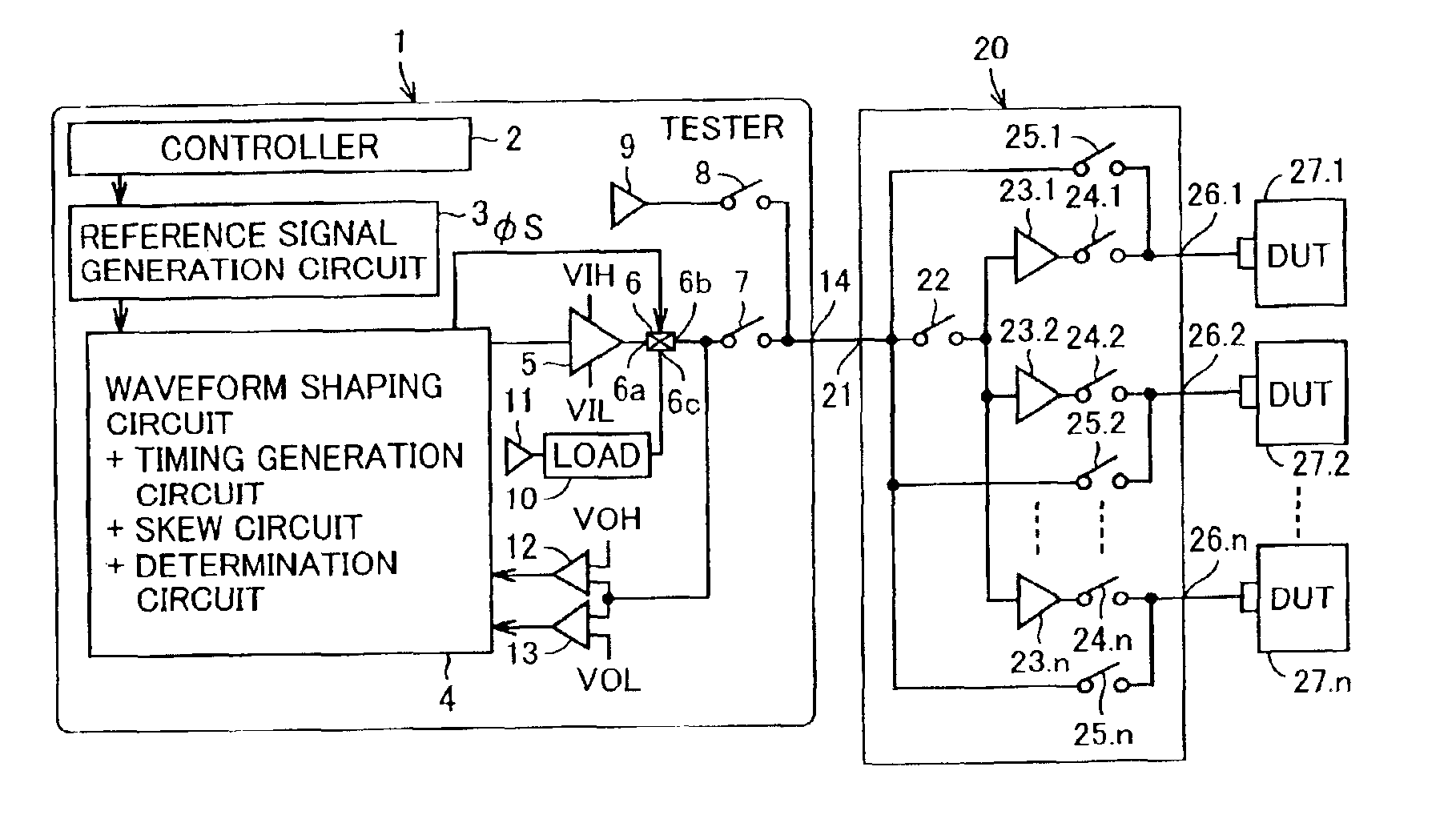
[0029]FIG. 1 is a circuit block diagram showing a main part of a semiconductor test system in accordance with a first embodiment of the present invention. In FIG. 1, this semiconductor test system includes a tester 1 and an interface circuit 20. Tester 1 includes a controller 2, a reference signal generation circuit 3, a test circuit 4, an output buffer 5, a fast change-over switch 6, switches 7, 8, a current measuring unit 9, a load circuit (LOAD) 10, a power supply for load circuit 11, comparators 12, 13, and an external pin 14. FIG. 1 only shows one external pin 14 of tester 1 and a part corresponding thereto. Actually, a number of external pins 14 are provided.

[0030]Controller 2 outputs a variety of control signals at a prescribed timing and controls the entire tester 1. Reference signal generation circuit 3 is controlled by controller 2 and outputs a reference signal. Test circuit 4 includes a waveform shaping circuit, a timing generation circuit, a skew circuit, and a determin...


PUM


Abstract

The interface circuit includes n buffer circuits, switches for connecting an external pin of a tester to input nodes of n buffer circuits and connecting output nodes of n buffers respectively to n DUTs when a signal is provided from the tester to n DUTs, and successively connecting n DUTs to the external pin of the tester by a prescribed time period when voltage-ampere characteristics of n DUTs are measured. Therefore the number of devices that can be measured by the tester at a time can be increased by n times. As a result, the test cost can be reduced and the test accuracy can be improved.

Description

BACKGROUND OF THE INVENTION[0001]1. Field of the Invention[0002]The present invention relates to an interface circuit, and more particularly to an interface circuit coupling a semiconductor test apparatus with a tested semiconductor device.[0003]2. Description of the Background Art[0004]Conventionally, in the field of semiconductor integrated circuit devices (referred to as LSI hereinafter), a test is performed before shipment to determine whether or not each LSI is normal and only a normal LSI is shipped. In this test, a plurality of LSIs are connected to one semiconductor test apparatus (referred to as a tester hereinafter). Usually, one external terminal of LSI is connected to one external pin of the tester, and a signal is applied, for example, from the external pin of the tester to the external terminal of LSI.[0005]In order to reduce the test cost for LSI, a method of connecting an output pin of a tester to a plurality of LSIs in parallel has been proposed (for example, see Ja...

Claims


Application Information

Patent Timeline
Patent Type & Authority Patents(United States)
IPC IPC(8): G01R31/319G01R31/28H03K19/0175
CPCG01R31/31926G01R31/31924G01R31/28
Inventor SUGIMOTO, MASARUFUNAKURA, TERUHIKONAGASAWA, HIDEKAZU
Owner RENESAS ELECTRONICS CORP
Why Eureka
Try Eureka