

Silicon-on-sapphire display apparatus and method of fabricating same
a display apparatus and silicon layer technology, applied in non-linear optics, instruments, optics, etc., can solve the problems of crystallographic defects, limited integration of display driving circuitry heretofore, and restricted display to reflective mode schemes
- Summary
- Abstract
- Description
- Claims
- Application Information
AI Technical Summary
Problems solved by technology
Method used
Image

Examples
Embodiment Construction
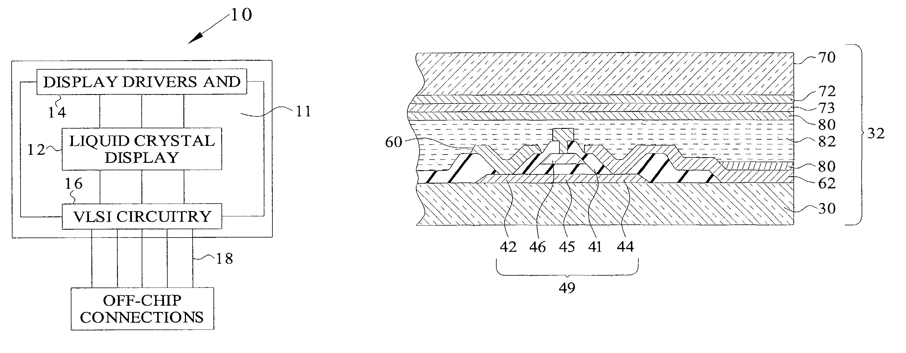
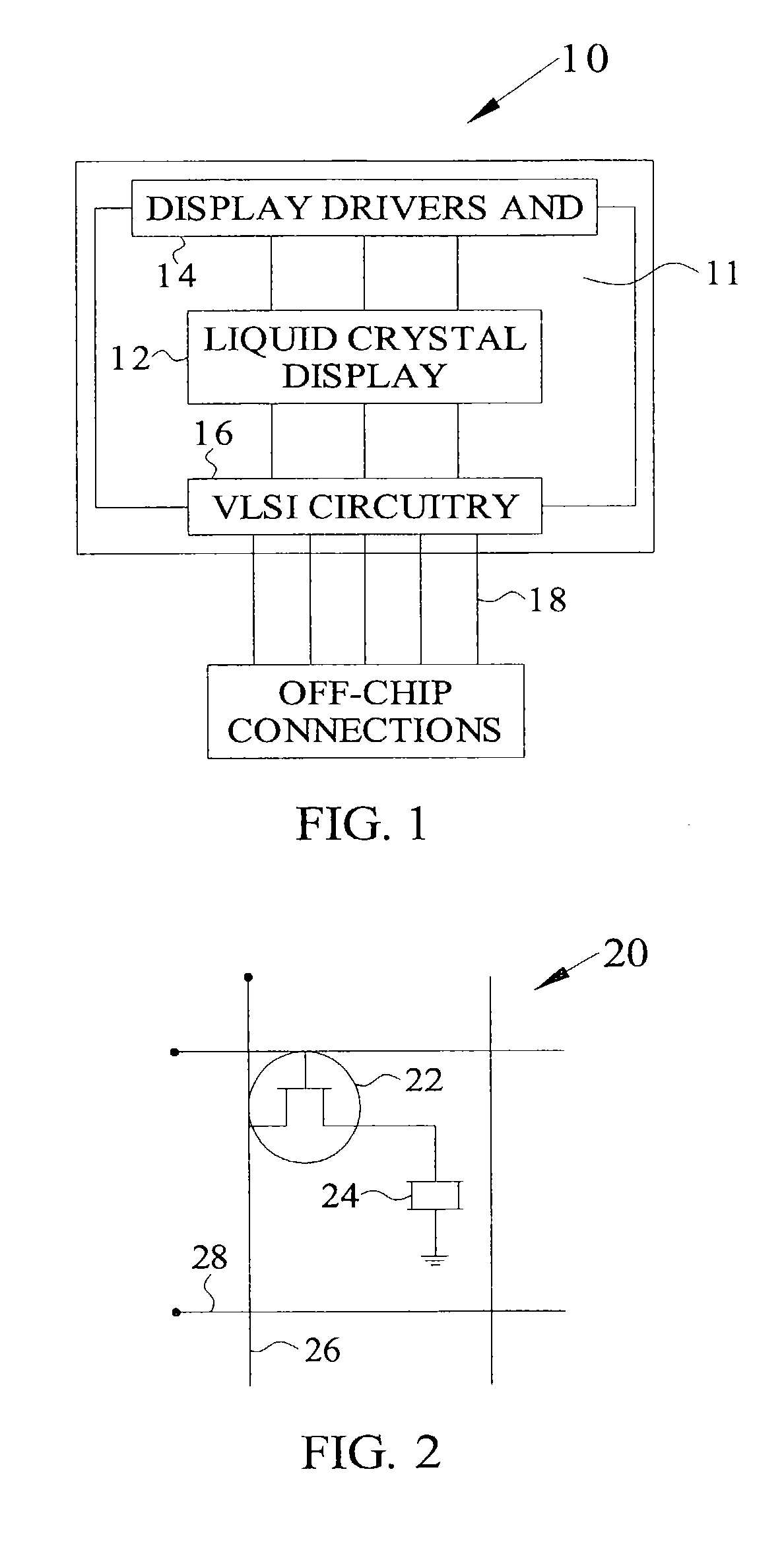
[0013]FIG. 1 schematically shows a top view of a display system 10 having a nematic liquid crystal display 12 monolithically integrated with associated circuitry 14 and 16 on an improved, ultra-thin silicon-on-sapphire (UTSOS) wafer. Display drivers 14 and very large scale integration (VLSI) circuitry 16 are used to address each of the individual pixels 20 and to apply appropriate voltages to modulate liquid crystal capacitor 24 to represent an image presented by liquid crystal display 12. Typically, display drivers 14 include shift registers, and clock circuitry. VLSI circuitry 16 may include image processing circuits, memory and buffer circuits, wireless interconnect circuitry and the like. A display area 12 in display or light valve system 10 has an array of one or more pixel elements which may be individually addressed so that display 12 presents an image for viewing or projection. By way of example, a 1000 pixel×1000 pixel display is described by way of example only. However, i...
PUM
 Abstract
Description
Claims
Application Information