Single crystal cutting method

a single crystal and cutting technology, applied in the direction of crystal growth process, polycrystalline material growth, manufacturing tools, etc., can solve the problems of unavoidable slicing loss of about 200 m per wafer, damaged layer at the sliced surface, and generated raw material loss, etc., to achieve good slicing surface and reduce slicing loss

Inactive Publication Date: 2005-10-25
SHIN-ETSU HANDOTAI CO LTD
View PDF5 Cites 52 Cited by
  • Summary
  • Abstract
  • Description
  • Claims
  • Application Information

AI Technical Summary

Benefits of technology

[0007]Therefore, the major object of the present invention is to provide a method for slicing a single crystal by using a laser, in which a single crystal is sliced while obtaining a good sliced surface and markedly reducing slicing loss.

Problems solved by technology

However, since stock removal for slicing is required when silicon wafers are sliced by using these apparatuses, there are generated loss of the raw material.
Even using a wire saw, which generates comparatively little slicing loss, slicing loss for about 200 μm per wafer is unavoidable.
Further, the slicing by a wire saw, inner diameter slicer or the like leaves a damaged layer at a sliced surface after the slicing.
Therefore, lapping, etching and so forth for removing the damaged layer are required, and they also generate loss of raw material.
Furthermore, in such a mechanical processing, if a wafer is sliced with an unduly small thickness from the raw material ingot, it becomes likely that the wafer breaks during the processing.
Therefore, a significant portion of the expensive single crystal material is wasted vainly.
However, the laser processing has a problem concerning melting due to evolution of heat or the like, and thus it suffers from disadvantages that peripheral portions under slicing are degraded and processing traces are remained.
Therefore, it has been difficult to apply the laser processing to the semiconductor processing, which requires processing precision less than micrometer order.
However, a slicing method utilizing such an ultra short pulse laser has problems, for example, atomic substances removed by the laser slicing reattach t o the processed surface and so forth, flatness of the sliced surface cannot be obtained and thus processed form is degraded.
Therefore, even if a laser slicing method utilizing an excimer laser or the like is applied as it is to the slicing of a single crystal such as a silicon single crystal, the advantage of the laser slicing that high speed and high efficiency processing is possible cannot be utilized effectively, and thus yield of the slicing of a single crystal cannot be improved compared with mechanical processing using a wire saw or inner diameter slicer.

Method used


Image

  • Single crystal cutting method
  • Single crystal cutting method
  • Single crystal cutting method

Examples


Embodiment Construction

[0031]Hereafter, embodiments of the present invention will be explained in detail.

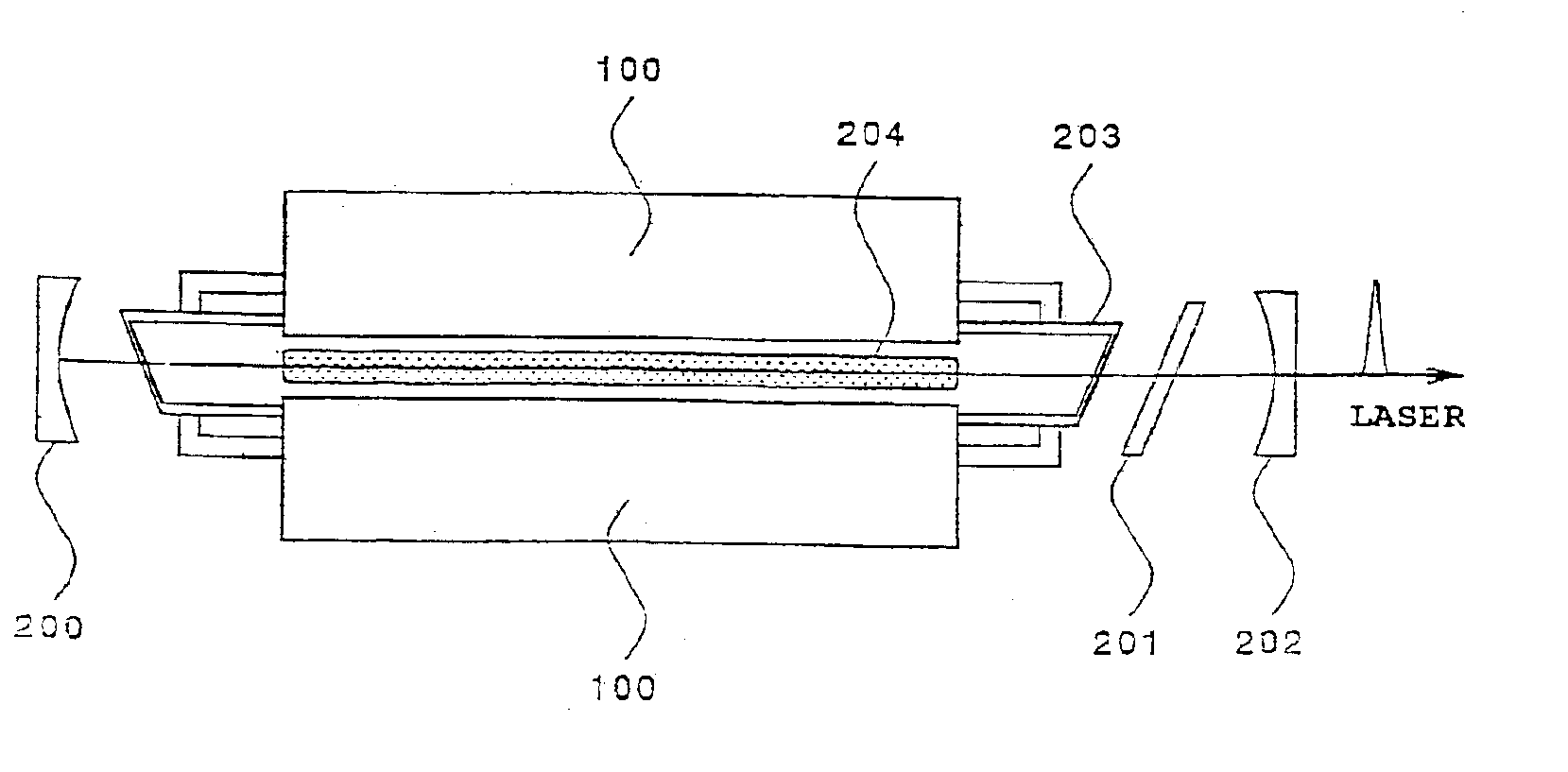
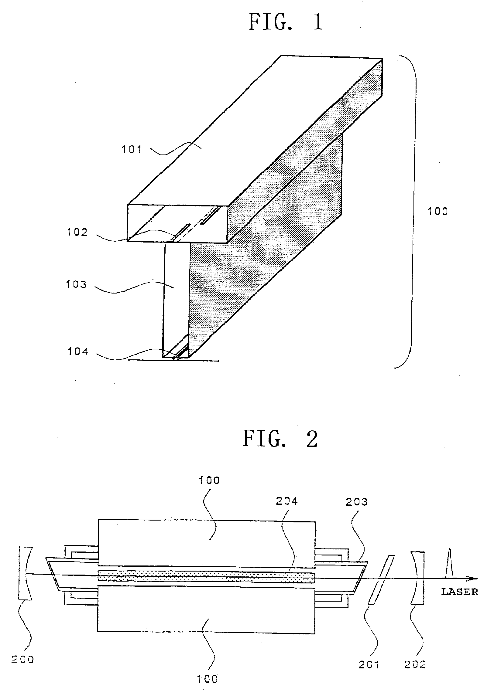
[0032]The inventors of the present invention conducted researches for a method that enables efficient utilization of a single crystal by slicing thin wafers from a single crystal such as a silicon single crystal with high precision and high efficiency. As described above, if a single crystal is sliced by using an ultra short pulse laser such as an excimer laser, atomic bonds themselves in the single crystal can be cut, and therefore processing only at the irradiated portion is possible with high precision. However, such laser processing has a problem that the removed atomic substances attach to the processed surface and the flatness of the processed surface is degraded.

[0033]Therefore, the inventors of the present invention conceived supplying a gas containing gaseous molecules or radicals that react with atomic substances removed by the processing to become stable gaseous molecules in the vicinity of ...


PUM

PropertyMeasurementUnit
anglesaaaaaaaaaa
resonator lengthaaaaaaaaaa
timeaaaaaaaaaa

Abstract

The present invention provides a method for slicing a single crystal, wherein the single crystal is sliced by irradiating a portion to be sliced with an ultra short pulse laser beam while supplying a gas containing gaseous molecules or radicals that react with atoms constituting the single crystal to become stable gaseous molecules in the vicinity of the portion under slicing. Thus, there is provided a method for slicing a single crystal by using a laser processing, in which a single crystal is processed while obtaining a good sliced surface and markedly reducing a slicing loss.

Description

TECHNICAL FIELD[0001]The present invention relates to a method for slicing a single crystal by using a laser, which can markedly reduce slicing loss and thereby enables effective use of the single crystal.BACKGROUND ART[0002]Single crystal wafers, of which typical examples are those of silicon (Si) and gallium arsenide (GaAs), are obtained by slicing a single crystal ingot produced by the Czochralski method (CZ method) or the floating zone method (FZ method) into wafers. Therefore, it is desired to obtain wafers as many as possible from one ingot by making thickness of wafer as small as possible or reducing the stock removal for slicing. That is, desirability of reducing thickness of wafers or processing loss in the production of wafers to reduce waste of the raw material and thereby reduce production cost of wafers has hitherto been widely recognized.[0003]For example, as an apparatus for slicing silicon wafers from a silicon single crystal ingot, a wire saw and inner diameter slic...

Claims


Application Information

Patent Timeline
Patent Type & Authority Patents(United States)
IPC IPC(8): B23K26/00B23K26/40B23K26/12B28D1/22H01L21/02H01L21/304B23K26/38
CPCB23K26/0635B23K26/12B23K26/123B23K26/4075B28D1/221H01L21/304B23K26/0057B23K26/127B23K2201/40B23K26/40B23K26/0624B23K26/53B23K2101/40B23K2103/50
Inventor OHMI, TADAHIROSUGAWA, SHIGETOSHISHINOHARA, TOSHIKUNIITO, TATSUOKANAYA, KOICHI
Owner SHIN-ETSU HANDOTAI CO LTD
Why Eureka
Try Eureka