Process for the back-surface grinding of wafers

a back-surface grinding and wafer technology, applied in the direction of polyether adhesives, film/foil adhesives, manufacturing tools, etc., can solve the problems of wafer breaking, no longer being able to contact the substrate surface, and not being able to complete contact with the substrate surfa

Inactive Publication Date: 2005-10-25
POLARIS INNOVATIONS LTD
View PDF25 Cites 12 Cited by
  • Summary
  • Abstract
  • Description
  • Claims
  • Application Information

AI Technical Summary

Problems solved by technology

The conventional films are no longer able to compensate for these differences in topography, and consequently contact with the substrate surface is not complete, and in particular the film rear side, which rests on the base during grinding of the wafer back surface, is no longer planar, but rather has undulations.
The grinding process then leads to local fluctuations in thickness (dimples) in the thinned wafers, which may cause the wafer to break.
If the contact bumps are larger than this, the drawbacks which have been described above occur.
Hitherto, there have been no leveling protective films which allow the back-surface grinding of wafers with larger contact bumps.
This process is likewise not suitable for the back-surface grinding of wafers which on their front surface have contact bumps or other structures with a height of more than 150 μm, since in this case too the abovementioned drawbacks occur.

Method used


Image

  • Process for the back-surface grinding of wafers
  • Process for the back-surface grinding of wafers

Examples


examples

[0052]1. Film with a First-Order Hybrid System

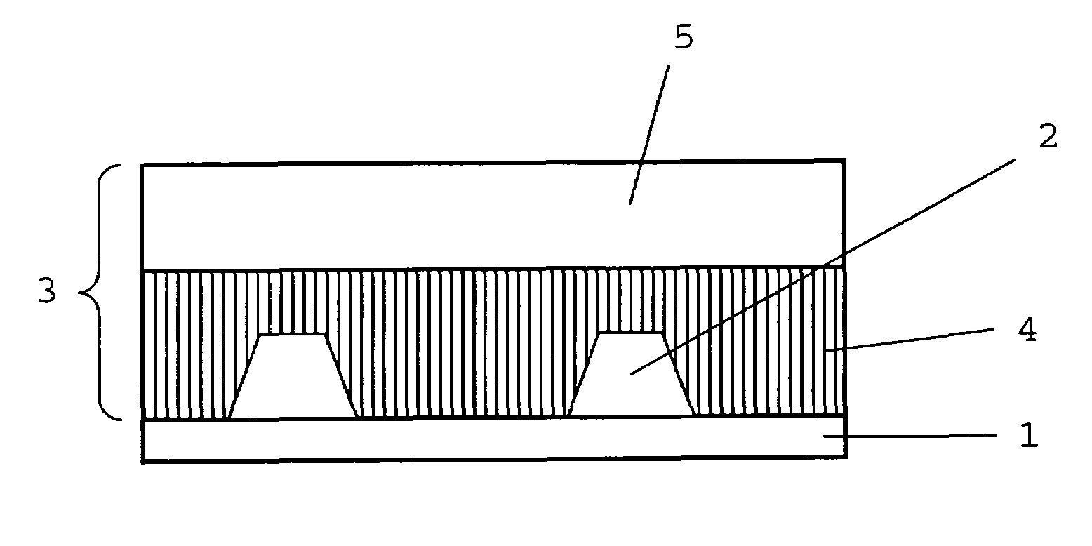
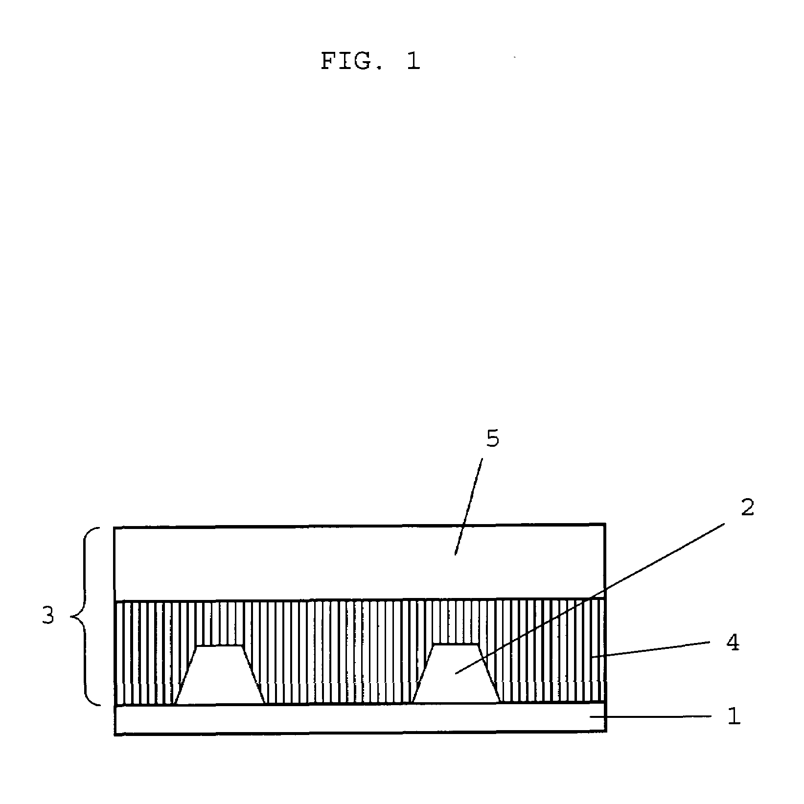
[0053]A pressure-exerting roller was used to laminate films onto wafers with a diameter of 200 or 300 mm and integrated circuits and contact bumps with a height of 250 μm (polymer or metal bumps) and a diameter of 400 μm situated thereon. The films had a support layer which was 150 μm thick and comprised polyolefins or PVC. The adhesion layer of the film had the following composition: 77.5% by weight of linear polyesters and 19.5% by weight of a triacrylate (TMPTA) as crosslinking constituent in combination with 2% by weight of benzoin and 1% by weight of benzoylperoxide. The layer thickness of the adhesion layer was 300 μm.

[0054]There followed a first photochemically initiated partial polymerization, which was controlled by means of the radiation intensity or time in such a way that the adhesion layer adopted an elastic behavior.

[0055]Then, the support rear side was positioned on a rotating vacuum chuck, which is part of the grinding ma...


PUM

PropertyMeasurementUnit
diameteraaaaaaaaaa
heightaaaaaaaaaa
thicknessaaaaaaaaaa

Abstract

The present invention relates to a process for the back-surface grinding of wafers using films which have a support layer, which is known per se, and an adhesion layer which can be polymerized in steps, and to films which include such an adhesion layer which can be polymerized in steps, and to the use thereof.

Description

RELATED APPLICATIONS[0001]This application is a continuation of PCT patent application number PCT / EP02 / 04776, filed Apr. 30, 2002, which claims priority to German patent application number 10121556.8, filed May 3, 2001, the disclosures of each of which are incorporated herein by reference in their entirety.TECHNICAL FIELD[0002]The present invention relates to a process for the back-surface grinding of wafers using films which have a support layer, which is known per se, and an adhesion layer which can be polymerized in steps, and to films which include such an adhesion layer which can be polymerized in steps, and to the use thereof.BACKGROUND ART[0003]Currently, during the back-surface grinding of semi-conductor wafers, protective films are adhesively bonded to the wafer front surface, and the wafer which has been covered in this way is placed, by means of the applied film, onto a flat base, and then the wafer back surface is ground, typically using a diamond abrasive. The protectiv...

Claims


Application Information

Patent Timeline
Patent Type & Authority Patents(United States)
IPC IPC(8): C09J167/00C09J171/00C09J175/04C09J7/02C09J163/00C09J133/00C09J11/02C09J11/06H01L21/67H01L21/70H01L21/30H01L21/68H01L21/302H01L21/02H01L21/00H01L21/58H01L21/304H01L21/461H01L21/78B24B7/22B24B41/06H01L
CPCB24B7/228B24B41/06H01L21/304H01L21/6836H01L2221/68327
Inventor ROGALLI, MICHAELSCHNEEGANS, MANFRED
Owner POLARIS INNOVATIONS LTD
Why Eureka
Try Eureka