Method for making silicon containing dielectric films

a dielectric film and silicon carbide technology, applied in the direction of electrical discharge tubes, semiconductor devices, electrical apparatus, etc., can solve the problems of difficult to effectively form an oxide layer on a sic semiconductor, additional many time-consuming (3–4 hour) wet ambient process, etc., to achieve the effect of effective forming an oxide layer and faster oxidation ra

Inactive Publication Date: 2005-11-22
UNIV OF SOUTH FLORIDA
View PDF4 Cites 9 Cited by
  • Summary
  • Abstract
  • Description
  • Claims
  • Application Information

AI Technical Summary

Benefits of technology

[0012]What is needed, then, is an improved method for effectively forming an oxide layer on a SiC semiconductor. The i

Problems solved by technology

It is difficult to effectively form an oxide layer on a SiC semiconductor.
In addition, following the ox

Method used


Image

  • Method for making silicon containing dielectric films
  • Method for making silicon containing dielectric films

Examples


Embodiment Construction

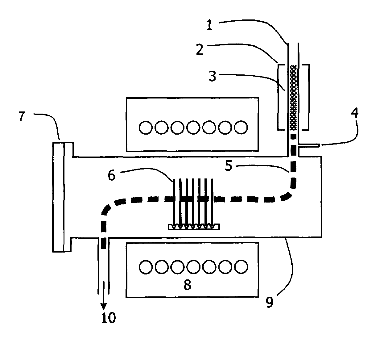
[0025]Referring now to FIG. 1, it will there be seen that an illustrative embodiment of the invention is depicted in diagrammatic form.

[0026]Silicon carbide substrate 6 is introduced into tube 9 through loading port 7. Furnace 8 encircles tube 9 so that the temperature within tube 9 may be controlled. Pump 10 is in fluid communication with tube 9 so that the pressure within tube 9 may be controlled. An oxidizing gas 1 is passed through an afterglow source such as a microwave cavity 2 so that gas 1 achieves an excited state of energy 3 or plasma phase that upon its exit from said cavity is in a neutral state. Afterglow species 5 then contacts substrate 6 within tube 9 which functions as an afterglow vessel. Furnace 8 maintains tube 9 and hence substrate 6 at a temperature between 600° C. to 1,200° C. and pump 10 maintains said tube at a pressure less than 50 torr.

[0027]More particularly, silicon carbide substrate 6 is supported within fused silica tube 9, or any appropriate vessel su...


PUM


Abstract

Method and apparatus for forming thin silicon oxide films on silicon carbide substrates utilizing an afterglow thermal reactor. The method of forming thin silicon oxide film includes the steps of loading a silicon carbide substrate within a tube, which tube is heated, and the contents pressure is controlled. An oxidizing gas is then passed through an afterglow reactor source or microwave cavity where the gas achieves an excited state of energy. When the neutral species of the excited gas contact the silicon carbide substrate within the heated region of the the tube, a thin silicon oxide film forms on the substrate, at a faster rate and lower temperature than has been known. The tube contents are maintained at a temperature between 600° C. to 1,200° C., and at a pressure less than 50 torr.

Description

CROSS-REFERENCE TO RELATED DISCLOSURE[0001]This disclosure claims priority from a provisional application entitled “Method of Forming Thin Silicon Films on Silicon Carbide Substrates,” filed Oct. 11, 2002 by the present inventor and bearing application No. 60 / 319,607.BACKGROUND OF INVENTION[0002]1. Field of the Invention[0003]This invention relates to growing thin films on silicon carbide substrates.[0004]2. Background of the Invention[0005]Metal-oxide-semiconductor are structures which include a silicon-carbide(SiC) substrate and an oxide film grown on the silicon-carbide (SiC) substrate. MOS diodes, MOSFETs and MOSICs are formed on a silicon carbide substrate and used in the art.[0006]Silicon Carbide (SiC) takes various kinds of crystal structures (referred to as polytype), and has a band gap between 2.4 eV and 3.3 eV depending on the crystal structure. The silicon carbide is thermally, chemically and physically stable, and resistant to high-energy particle radiation. Accordingly,...

Claims


Application Information

Patent Timeline
IPC IPC(8): H01L21/469H01L21/02H01L21/31H01L21/04
CPCH01J37/32192H01L21/049Y10S438/906
Inventor HOFF, ANDREW M.
Owner UNIV OF SOUTH FLORIDA
Why Eureka
Try Eureka