Impedance-matched output driver circuits having enhanced predriver control

a driver circuit and predriver technology, applied in logic circuits, pulse techniques, reliability increasing modifications, etc., can solve the problems of relatively large transistors, relatively high output capacitance, and limited speed of the driver circuit b>10/b>, and achieve the effect of improving the operating characteristics

Active Publication Date: 2005-11-22
INTEGRATED DEVICE TECH INC
View PDF51 Cites 10 Cited by
  • Summary
  • Abstract
  • Description
  • Claims
  • Application Information

AI Technical Summary

Benefits of technology

[0008]Impedance-matched output driver circuits according to embodiments of the present invention utilize predriver circuits with analog impedance control to provide enhanced operating characteristics. Moreover, because the impedance control is provided by a predriver circuit, the control circuitry does not affect the output driver size. This analog control may be provided by an analog loop containing differential amplifiers that set the resolution limit of the output driver circuit. These output driver circuits include a first PMOS pull-up transistor having source and drain terminals electrically connected in series in a pull-up path of the output driver circuit. An NMOS pass transistor is also provided. The NMOS pass transistor has a first current carrying terminal (e.g., drain) electrically connected to a gate terminal of the first PMOS pull-up transistor and a second current carrying terminal (e.g., source) configured to receive a P-type reference voltage (VP). This P-type reference voltage controls the conductivity of the first PMOS pull-up transistor in the pull-up path. A gate terminal of the NMOS pass transistor is responsive to a pull-up data input signal (DINP). Accordingly, when the pull-up data input signal is set high, the NMOS pass transistor operates to pull down the gate terminal of the first PMOS pull-up transistor to a level set by the P-type reference voltage.

Problems solved by technology

Furthermore, the speed of the driver circuit 10 may be limited by the fact that both the pull-up and pull-down paths include a serial connection of two transistors, which means that relatively large transistors are required to maintain sufficiently high switching speed.
However, because two of the transistor gates are connected to the output terminal OUT, the driver circuit 12 of FIG. 3 may have relatively poor electrostatic discharge (ESD) characteristics and relatively high output capacitance.

Method used


Image

  • Impedance-matched output driver circuits having enhanced predriver control
  • Impedance-matched output driver circuits having enhanced predriver control
  • Impedance-matched output driver circuits having enhanced predriver control

Examples


Embodiment Construction

[0022]The present invention now will be described more fully herein with reference to the accompanying drawings, in which preferred embodiments of the invention are shown. This invention may, however, be embodied in many different forms and should not be construed as being limited to the embodiments set forth herein; rather, these embodiments are provided so that this disclosure will be thorough and complete, and will fully convey the scope of the invention to those skilled in the art. Like reference numerals refer to like elements throughout and signal lines and signals thereon may be referred to by the same reference characters. Signals may also be synchronized and / or undergo minor boolean operations (e.g., inversion) without being considered different signals.

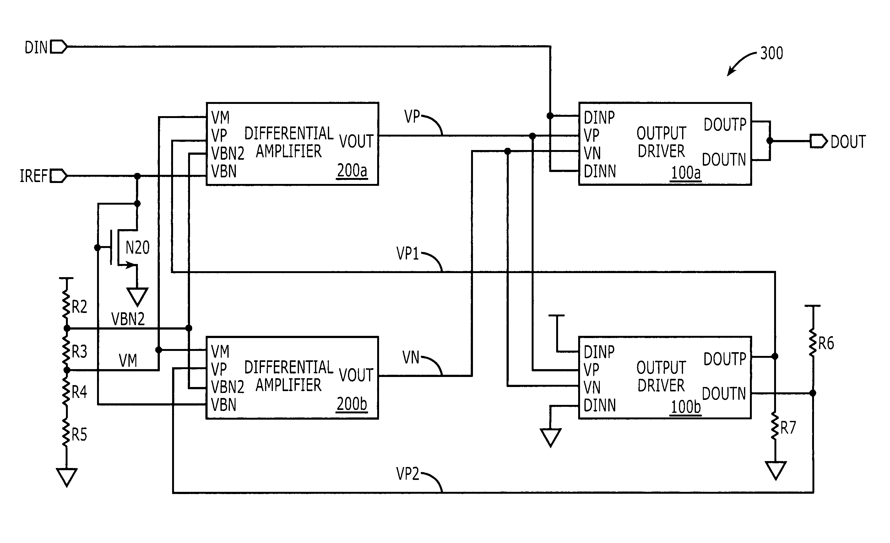
[0023]Referring now to FIG. 4, an output driver circuit 100 according to an embodiment of the present invention is configured to receive a pair of data input signals DINP and DINN and generate a pair of data output signals D...


PUM


Abstract

Impedance-matched output driver circuits utilize predriver circuits with analog control to provide enhanced operating characteristics. This analog control may be provided by an analog loop containing differential amplifiers that set the resolution limit of the output driver circuit. These output driver circuits include a first PMOS pull-up transistor having source and drain terminals electrically connected in series in a pull-up path of the output driver circuit. An NMOS pass transistor has a first current carrying terminal electrically connected to a gate terminal of the first PMOS pull-up transistor and a second current carrying terminal configured to receive a P-type analog reference voltage (VP). This P-type reference voltage controls the conductivity of the first PMOS pull-up transistor in the pull-up path. A gate terminal of the NMOS pass transistor is responsive to a pull-up data input signal (DINP). A first NMOS pull-down transistor has source and drain terminals that are electrically connected in series in a pull-down path of the output driver circuit. A PMOS pass transistor is provided having a first current carrying terminal electrically connected to a gate terminal of the first NMOS pull-down transistor and a second current carrying terminal configured to receive an N-type analog reference voltage (VN). This N-type reference voltage controls the conductivity of the first NMOS pull-down transistor in the pull-down path. A gate terminal of the PMOS pass transistor is responsive to a pull-down data input signal (DINN).

Description

CROSS-REFERENCE TO RELATED APPLICATION[0001]This application is related to U.S. application Ser. No. 10 / 616,272, filed Jul. 9, 2003, the disclosure of which is hereby incorporated herein by reference.FIELD OF THE INVENTION[0002]The present invention relates to integrated circuit devices and, more particularly, to output driver circuits that drive off-chip loads.BACKGROUND OF THE INVENTION[0003]Output driver circuits are frequently configured to have impedance matching characteristics that enable off-chip loads to be driven more efficiently. FIG. 1 illustrates a conventional impedance-matched output driver circuit 10 having a totem pole arrangement of PMOS pull-up transistors and NMOS pull-down transistors therein. As illustrated, a pull-up path of the driver circuit 10 includes a plurality of PMOS pull-up transistors, shown as MP0 and MP1, and a pull-down path of the driver circuit 10 includes a plurality of NMOS pull-down transistors, shown as MN0 and MN1. The PMOS pull-up transist...

Claims


Application Information

Patent Timeline
Patent Type & Authority Patents(United States)
IPC IPC(8): H03K19/003H03K17/16H03K19/00H03K19/017
CPCH03K17/164H03K19/0005H03K19/0027H03K19/01721
Inventor BUTKA, BRIAN
Owner INTEGRATED DEVICE TECH INC
Why Eureka
Try Eureka