Redundancy architecture for repairing semiconductor memories

Inactive Publication Date: 2005-11-22
LONGITUDE SEMICON S A R L
View PDF8 Cites 84 Cited by
  • Summary
  • Abstract
  • Description
  • Claims
  • Application Information

AI Technical Summary

Benefits of technology

[0036]Therefore, an object of the present invention is to provide a redundancy architecture f

Problems solved by technology

However, the use of the laser beams for programming the fuses requires blowing the fuses before packaging semiconductor memories into packages.
This means that the semiconductor memories are not repairable after packaging, and thus the product yield is not effectively improved.
The use of a nonvolatile memory, however, increases a chip size of a semiconductor memory, because a nonvolatile memory requires a wider area per bit than a fuse circuitry.
A drawback of the conventional repairing process is that considerable costs are required for testing and repairing many semiconductor memories concurrently.
To test and repair a plura

Method used


Image

  • Redundancy architecture for repairing semiconductor memories
  • Redundancy architecture for repairing semiconductor memories
  • Redundancy architecture for repairing semiconductor memories

Examples


Embodiment Construction

[0067]The present invention will be described below in detail with reference to the attached drawings.

Memory Device Structure

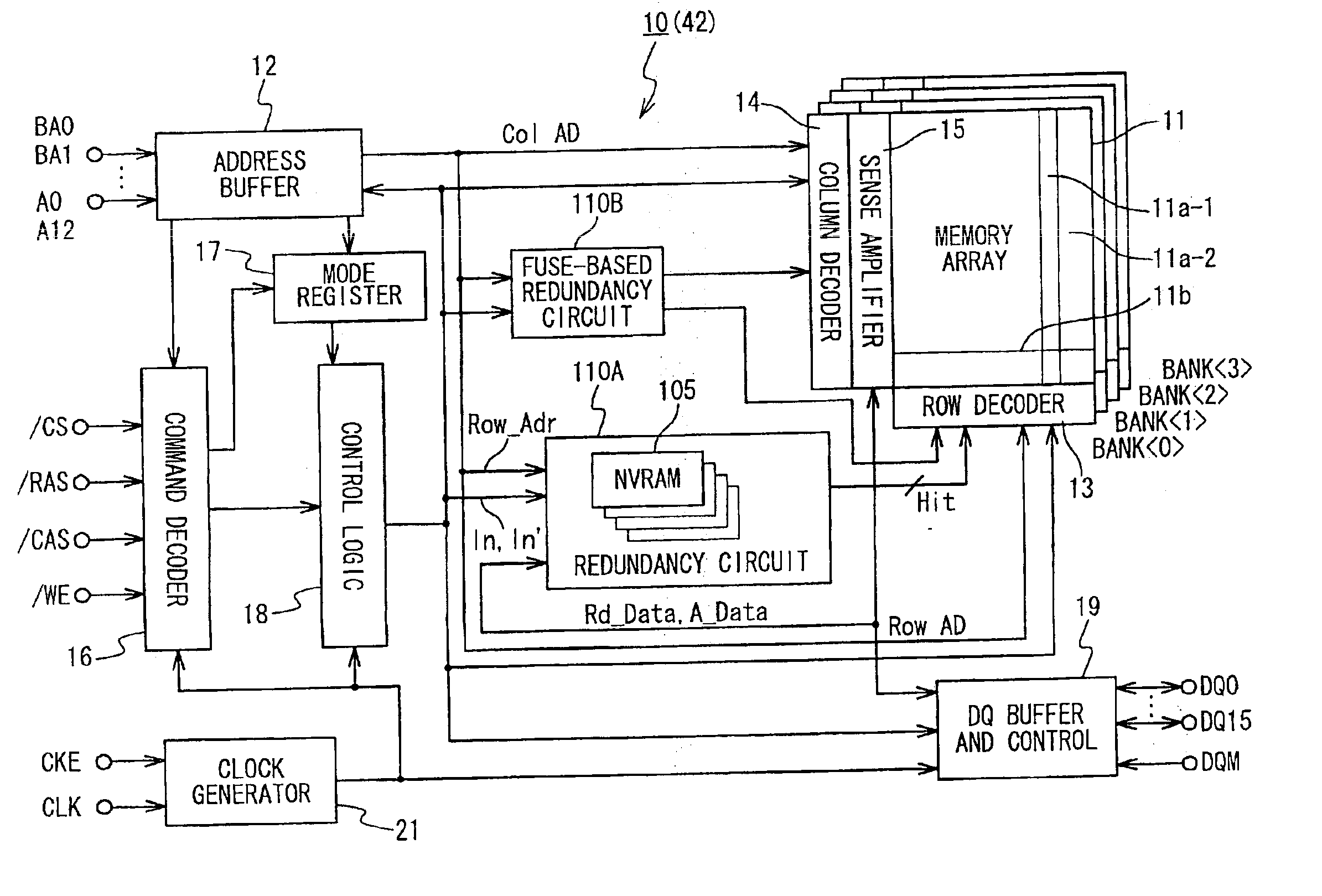
[0068]FIG. 4 shows a block diagram of a monolithic SDRAM 10 provided on a memory chip 42 including a redundancy architecture in accordance with the present invention. It should be noted that an element shown in FIG. 4 and its corresponding elements shown in FIG. 3 are denoted by the same numeral to represent that they have a substantially identical function, and thus a detailed explanation thereof may be omitted.

[0069]The SDRAM 10 includes a memory cell array 11, an address buffer 12, a command decoder 16, a mode register 17, a control logic circuit 18, a data input / output buffer 19, a clock generator 21, a NVRAM-based redundancy circuitry 110A, a fuse-based redundancy circuitry 110B.

[0070]The memory cell array 11 includes memory banks 0> to 3>, and each of the memory banks is provided with memory cells arranged in rows and columns, redundant cells, a row deco...


PUM


Abstract

A redundancy architecture for improving the throughput of testing and repairing the semiconductor memory after packaging. A memory device is composed of a memory cell array including memory cells and first redundant cells, a data comparator comparing read data received from the memory cell array with anticipated data provided by an external tester to produce a data mismatch signal, a redundancy mapping circuit responsive to the data mismatch signal for detecting a defective address of the memory cell array, a nonvolatile memory storing the detected defective address, and a redundancy circuitry repairing the memory cell array by replacing ones of the memory cells associated with the defective address with the first redundant cells.

Description

BACKGROUND OF THE INVENTION[0001]1. Field of the Invention[0002]The present invention relates, in general, to redundancy architecture for repairing semiconductor memories, and more particularly, to a redundancy architecture for improving a throughput of a test that includes repairing semiconductor memories.[0003]2. Description of the Related Art[0004]Redundancy is widely used in high-density semiconductor memories to improve product yield. As an example, a semiconductor memory may include redundant rows and columns, an address mapping circuit storing addresses of defective rows and columns, and a redundancy circuit for repairing defective rows and columns by redirecting the defective addresses to those of redundant rows and columns.[0005]Defective addresses are often stored in fuses that are programmable by blowing them with laser beams. However, the use of the laser beams for programming the fuses requires blowing the fuses before packaging semiconductor memories into packages. Thi...

Claims


Application Information

Patent Timeline
IPC IPC(8): G01R31/28G11C16/06G11C7/00G11C29/00H01L21/70H01L21/822H01L21/82H01L31/0328H01L31/0264H01L27/04G11C29/04G11C29/12
CPCG11C29/785G11C29/00
Inventor DONO, CHIAKI
Owner LONGITUDE SEMICON S A R L
Why Eureka
Try Eureka