Treatment method of film quality for the manufacture of substrates

a technology of film quality and substrate, applied in the field of manufacture of objects, can solve the problems of limiting the degree of integration achievable in a given chip, conventional isolation techniques consume a considerable amount of valuable wafer surface area on the chip, and the technique is not free from limitations, so as to improve the integrity of the bond interface, reduce defects, and improve the effect of crystal structur

Inactive Publication Date: 2005-11-29
SILICON GENERAL CORPORATION
View PDF45 Cites 109 Cited by
  • Summary
  • Abstract
  • Description
  • Claims
  • Application Information

AI Technical Summary

Benefits of technology

[0010]Numerous benefits are achieved by way of the present invention over pre-existing techniques. For example, the present invention provides an efficient technique for forming a substantially uniform surface on an SOI wafer. Additionally, the substantially uniform surface is made by way of common hydrogen treatment, deposition, and etching techniques, which can be found in conventional epitaxial tools. Furthermore, the present invention provides a novel uniform layer, which can be ready for the manufacture ...

Problems solved by technology

These techniques, however, are not free from limitations.
For example, conventional isolation techniques consume a considerable amount of valuable wafer surface area on the chip, and often generate a non-planar surface as an artifact of the isolation process.
Either or both of these considerations generally limit the degree of integration achievable in a given chip.
Additionally, trench isolation often requires a process of reactive ion etching, which is extre...

Method used


Image

  • Treatment method of film quality for the manufacture of substrates
  • Treatment method of film quality for the manufacture of substrates
  • Treatment method of film quality for the manufacture of substrates

Examples


Embodiment Construction

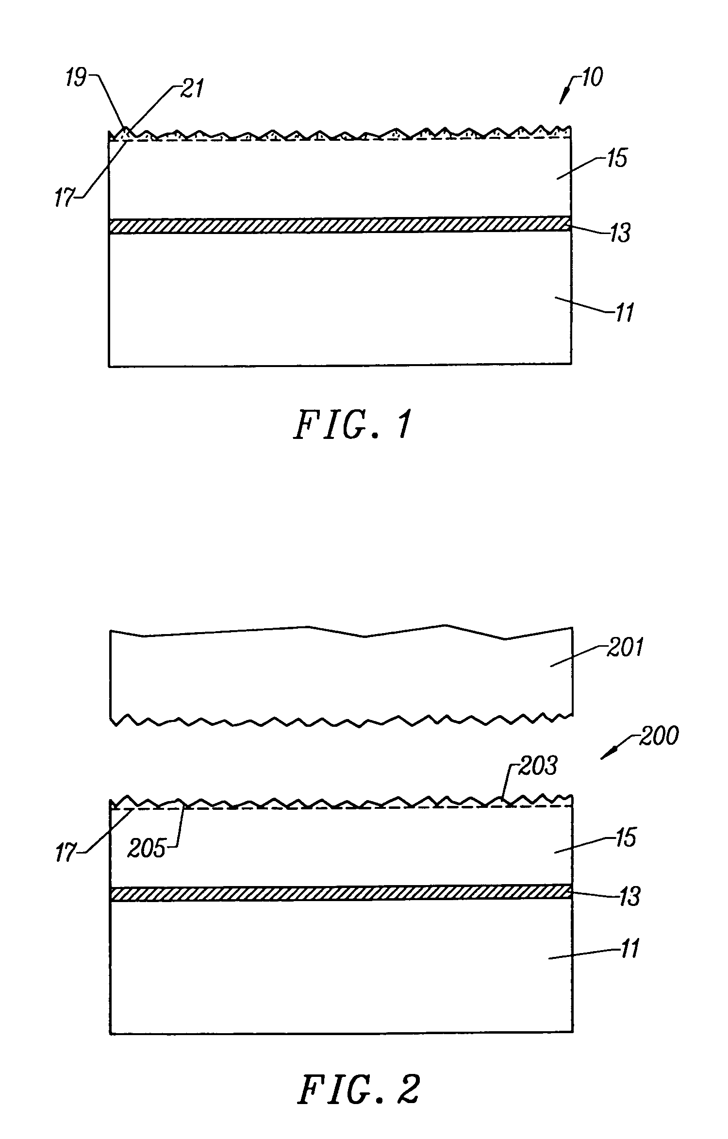
[0014]According to the present invention, a technique for treating a film of material is provided. More particularly, the present invention provides a method for treating a defective film using a combination of thermal treatment and chemical reaction, which can form a substantially smooth defect free film layer for the manufacture of integrated circuits, for example. The invention will be better understood by reference to the Figs. and the descriptions below.

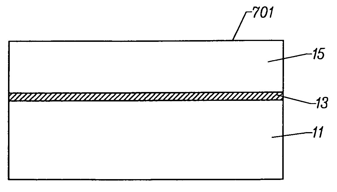
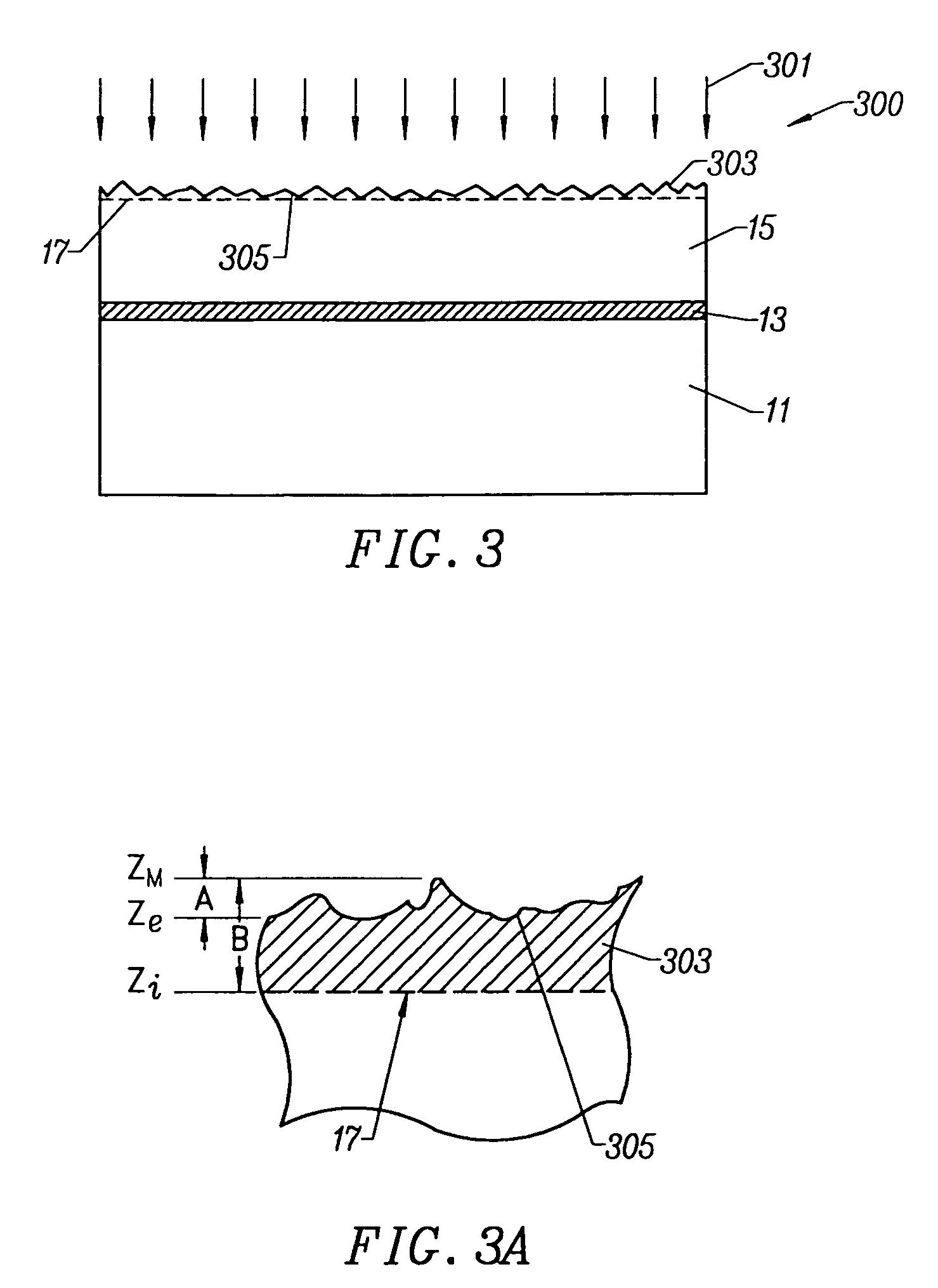
[0015]FIG. 1 is a simplified cross-sectional view diagram of a substrate 10 according to the present invention. The diagram is merely an illustration and should not limit the scope of the claims herein. As merely an example, substrate 10 is a silicon wafer which includes a material region 12 to be removed, which is a thin relatively uniform film derived from the substrate material. The silicon wafer 10 includes a top surface 14, a bottom surface 16, and a thickness 18. Substrate 10 also has a first side (side 1) and a second sid...


PUM

PropertyMeasurementUnit
Temperatureaaaaaaaaaa
Sizeaaaaaaaaaa
Nanoscale particle sizeaaaaaaaaaa

Abstract

A method of fabricating substrates, e.g., bulk wafers, silicon on insulator wafers, silicon on saphire, optoelectronic substrates. The method includes providing a substrate (e.g., silicon, gallium arsenide, gallium nitride, quartz). The substrate has a film characterized by a non-uniform surface, which includes a plurality of defects. At least some of the defects are of a size ranging from about 100 Angstroms and greater. The method also includes applying a combination of a deposition species for deposition of a deposition material and an etching species for etching etchable material. The combination of the deposition species and the etching species contact the non-uniform surface in a thermal setting to reduce a level of non-uniformity of the non-uniform surface by filling a portion of the defects to smooth the film of material. The smoothed film of material is substantially free from the defects and is characterized by a surface roughness of a predetermined value.

Description

CROSS-REFERENCES TO RELATED APPLICATIONS[0001]The present invention is a continuation of and claims priority to U.S. application Ser. No. 09 / 295,858 filed Apr. 21, 1999, now U.S. Pat. No. 6,171,965, commonly assigned and hereby incorporated by reference for all purposes.BACKGROUND OF THE INVENTION[0002]The present invention relates to the manufacture of objects. More particularly, the present invention provides a technique for improving surface texture or surface characteristics of a film of material, e.g., silicon, silicon germanium, or others. The present invention can be applied to treating or smoothing a cleaved film from a layer transfer process for the manufacture of integrated circuits, for example. The invention can also be applied to treating a film of material to fill a defect (e.g., hydrofluoric acid (“HF”) defect, pin hole, crystalline defect) in the film for the manufacture of integrated circuits, for example. But it will be recognized that the invention has a wider ran...

Claims


Application Information

Patent Timeline
IPC IPC(8): H01L21/302H01L21/304H01L21/3065H01L21/762
CPCH01L21/304H01L21/3065H01L21/76254H01L21/76259Y10S148/012
Inventor KANG, SIEN G.MALIK, IGOR J.
Owner SILICON GENERAL CORPORATION
Why Eureka
Try Eureka