

Stacked via-stud with improved reliability in copper metallurgy
a copper metallurgy and reliability technology, applied in the direction of layered products, transportation and packaging, chemistry apparatus and processes, etc., can solve the problems of increasing crack propensity, increasing crack generation, and increasing the proneness of stacked via-studs of present and future interconnection wiring schemes, so as to facilitate redundant paths and increase the flexibility of stacked via-studs
- Summary
- Abstract
- Description
- Claims
- Application Information
AI Technical Summary
Benefits of technology
Problems solved by technology
Method used
Image

Examples
Embodiment Construction
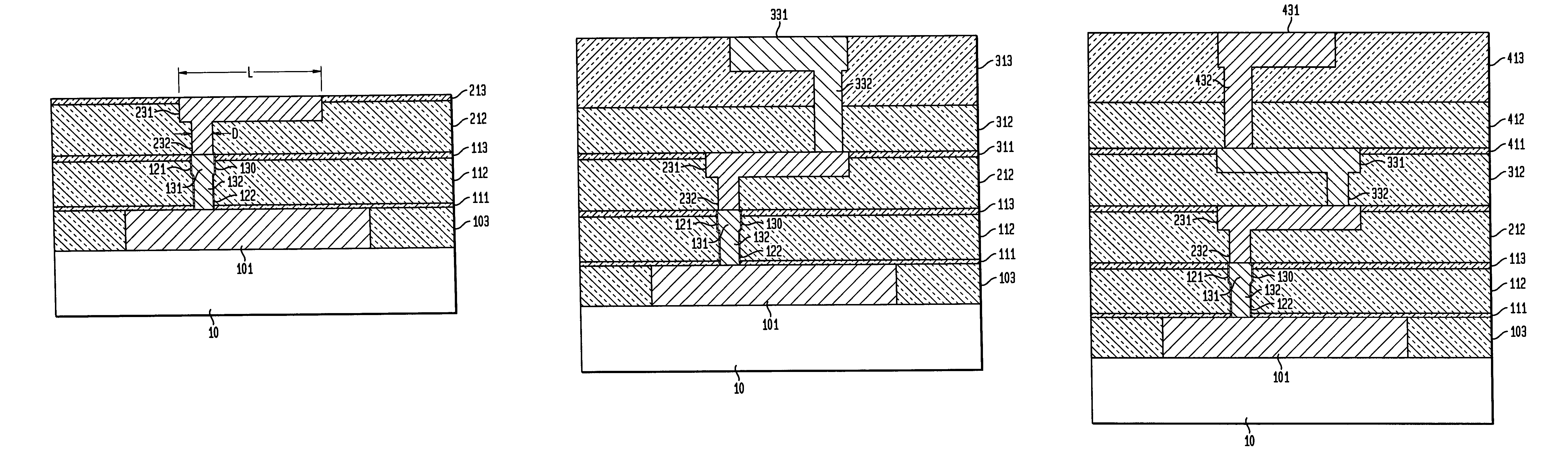
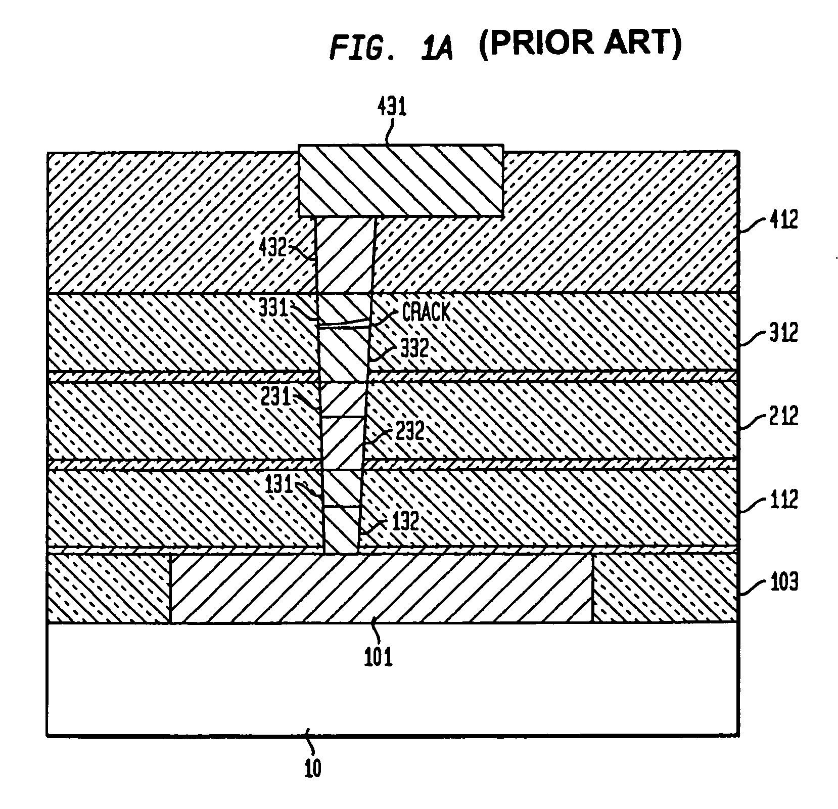
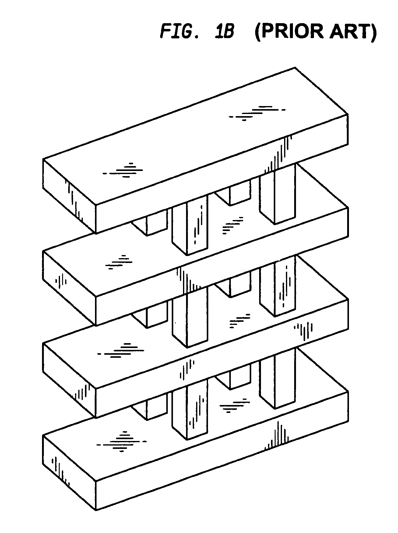
[0048]The present invention is generally related to methods for forming metal filled via-studs and conductor lines on a substrate where the via-studs and conductor lines are formed using a dual damascene method, and preferably copper metallurgy and low-k dielectric material. The present invention has particular relevance to stacked via-stud schemes which particularly use low strength low-k dielectric materials and incorporate a cantilever structure within the stacked via-stud which may serve as an effective thermal fatigue crack stop.
[0049]Particularly referring to FIG. 2, there is shown a semiconductor substrate 10 above which a sequence of dielectric layers 111, 112, 113 is deposited, subsequently patterned and metallized to form a first level of interconnection. It should be understood that a plurality of semiconductor devices may be formed in the substrate and, although not shown, are provided with a local interconnect line 101, typically tungsten with underlayers of titanium an...
PUM
| Property | Measurement | Unit |
|---|---|---|
| thickness | aaaaa | aaaaa |
| thickness | aaaaa | aaaaa |
| thickness | aaaaa | aaaaa |
Abstract
Description
Claims
Application Information