One-dimensional and two-dimensional electronically scanned slotted waveguide antennas using tunable band gap surfaces

Active Publication Date: 2005-12-06
ROCKWELL COLLINS INC
View PDF12 Cites 89 Cited by
  • Summary
  • Abstract
  • Description
  • Claims
  • Application Information

AI Technical Summary

Benefits of technology

[0013]It is an advantage of the present invention to apply electromagnetic crystal structures on sidewalls of a feed waveguide to provide phase shifting to scan a beam.
[0014]It is an advantage of the present invention to apply electromagnetic crystal structures on sidewalls of radiation waveguides

Problems solved by technology

Parallel feed antennas are unattractive for certain applications such as commercial weather radar since they suffer high weight and consume substantial volumetric real estate on the back side of the radiation aperture.
Antenna thickness is an issue for commercial aircraft since the nose radome swept volume requirement limits the aperture size due to the ±90° mechanical scanning requirement in azimuth.
It is essentially impractical to integrate PIN diode phase shifters within a series feed waveguide 17 d

Method used


Image

  • One-dimensional and two-dimensional electronically scanned slotted waveguide antennas using tunable band gap surfaces
  • One-dimensional and two-dimensional electronically scanned slotted waveguide antennas using tunable band gap surfaces
  • One-dimensional and two-dimensional electronically scanned slotted waveguide antennas using tunable band gap surfaces

Examples


Embodiment Construction

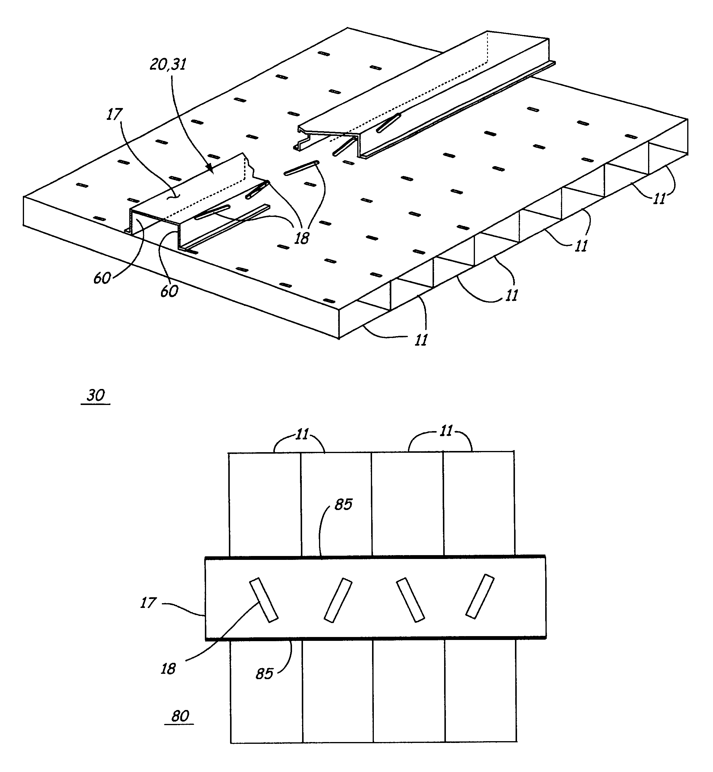
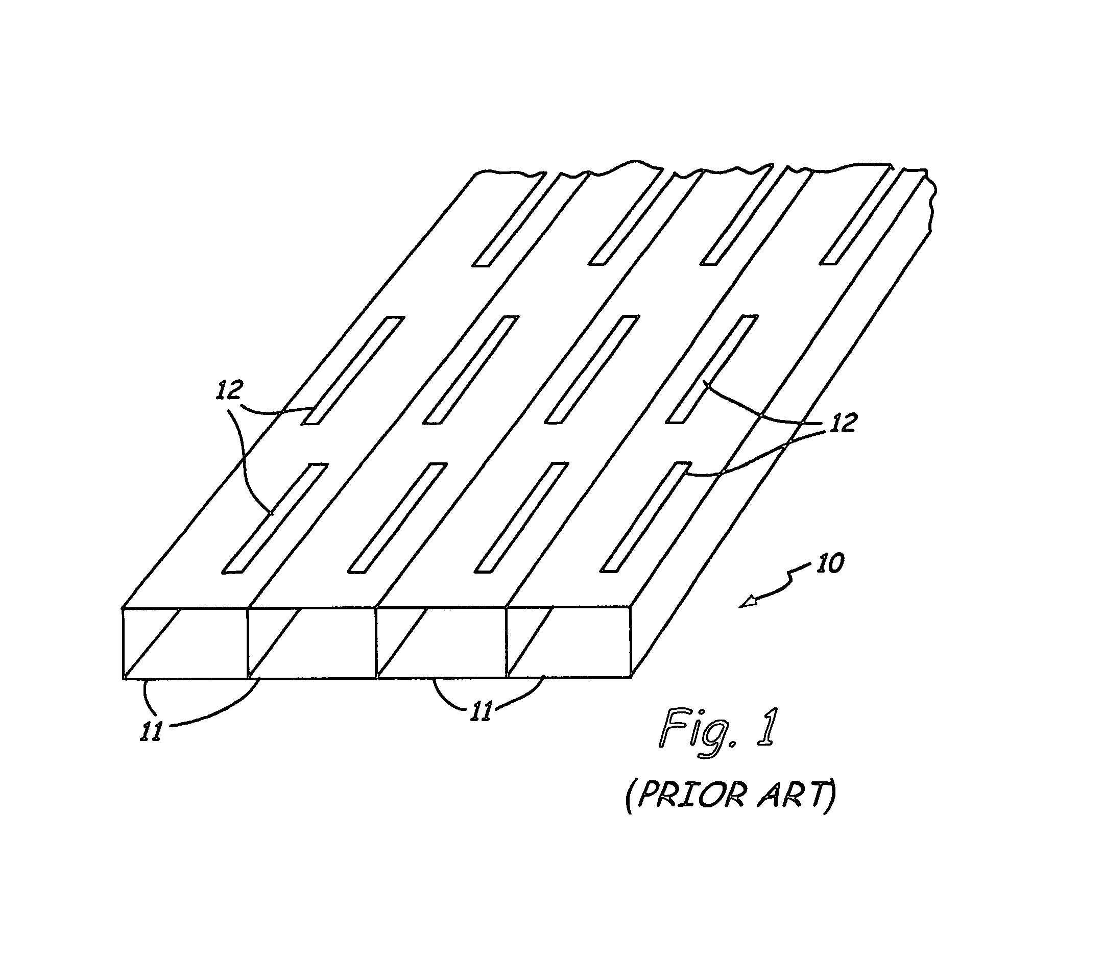
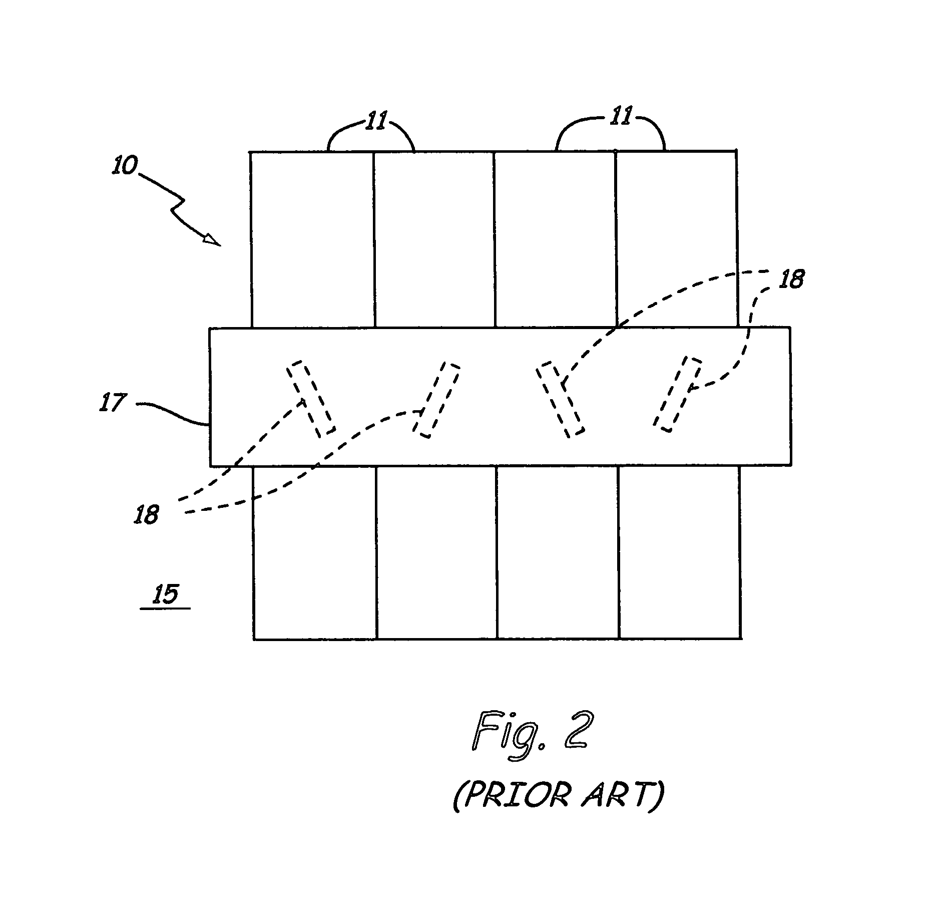
[0035]The invention described herein utilizes electromagnetic crystal (EMXT) lined waveguide sidewalls to achieve phase shifting required for electronic scanning of one-dimensional and two-dimensional slotted waveguide antennas.

[0036]EMXT devices are also known as tunable photonic band gap (PBG) and tunable electromagnetic band gap (EBG) substrates in the art. The Rockwell Scientific Company, Inc. (RSC) has developed waveguide phase shifting technologies that utilize tunable EBG substrates as waveguide walls. A detailed description of a waveguide section with tunable EBG phase shifter technologies is available in a paper by J. A. Higgins et al. “Characteristics of Ka Band Waveguide using Electromagnetic Crystal Sidewalls” 2002 IEEE MTT-S International Microwave Symposium, Seattle, Wash., June 2002. A typical EMXT structure 19, shown in FIG. 3, is described in the referenced paper. Other similar structures may be implemented based on design requirements. Electromagnetic band gap (EBG...


PUM


Abstract

An electronically scanned slotted waveguide antenna radiates an RF signal as a scannable beam. The antenna has radiation waveguides positioned in an array. Radiation slots in the radiation waveguides radiate the scannable beam. A feed waveguide is coupled to the radiation waveguides. The feed waveguide feeds the RF signal to the radiation waveguides through coupling slots. The feed waveguide has sidewalls with tunable electromagnetic crystal (EMXT) structures thereon. The EMXT structures vary the phase of the RF signal in the feed waveguide to scan the radiated beam in one dimension. The radiation waveguides may also have tunable EMXT structures on the sidewalls to vary the phase of the RF signal to scan the radiated beam in a second dimension. The EMXT structures may be discrete EMXT devices or a EMXT material layer covering the feed and radiation waveguide sidewalls.

Description

CROSS REFERENCE TO RELATED APPLICATIONS[0001]The present application is related to co-pending application Ser. No. 10 / 273,459 and filed on Oct. 18, 2002 entitled “A Method and Structure for Phased Array Antenna Interconnect” invented by John C. Mather, Christina M. Conway, and James B. West. The co-pending application is incorporated by reference herein in its entirety. All applications are assigned to the assignee of the present application.BACKGOUND OF THE INVENTION[0002]This invention relates to antennas, phased array antennas, and specifically to one- and two-dimensional electronically scanned slotted waveguide antennas using tunable photonic band gap structures.[0003]A slotted waveguide antenna array is very attractive for certain applications such as weather and fire control radar, where very high radiation efficiency and low cross-polarization levels are required. An overview of the basic design methodology for slotted waveguide arrays is presented in Johnson, R. C., and Jasi...

Claims


Application Information

Patent Timeline
IPC IPC(8): H01P1/18H01Q3/44H01Q13/22H01Q21/00
CPCH01P1/181H01P1/182H01P1/2005H01Q3/44H01Q21/0056
Inventor WEST, JAMES B.MATHER, JOHN C.LANDT, DON L.
Owner ROCKWELL COLLINS INC
Why Eureka
Try Eureka