MTJ stack with crystallization inhibiting layer

a technology of mtj stack and crystallization inhibiting layer, which is applied in the direction of digital storage, semiconductor devices, instruments, etc., to achieve the effects of improving coercitivity hc, cmos compatibility, and improving thermal stability

Inactive Publication Date: 2005-12-20
POLARIS INNOVATIONS
View PDF9 Cites 132 Cited by
  • Summary
  • Abstract
  • Description
  • Claims
  • Application Information

AI Technical Summary

Benefits of technology

[0010]Advantages of preferred embodiments of the present invention include providing a resistive memory element and method of manufacture thereof having improved thermal stability, improved coercitivity Hc, and CMOS compatibility. The crystallization inhibiting layer advantageously may also function as a diffusion barrier.

Problems solved by technology

Because MRAM devices operate differently than traditional memory devices and because they are relatively new, they introduce design and manufacturing challenges.

Method used


Image

  • MTJ stack with crystallization inhibiting layer
  • MTJ stack with crystallization inhibiting layer
  • MTJ stack with crystallization inhibiting layer

Examples


Embodiment Construction

[0021]The making and using of the presently preferred embodiments are discussed in detail below. It should be appreciated, however, that the present invention provides many applicable inventive concepts that can be embodied in a wide variety of specific contexts. The specific embodiments discussed are merely illustrative of specific ways to make and use the invention, and do not limit the scope of the invention.

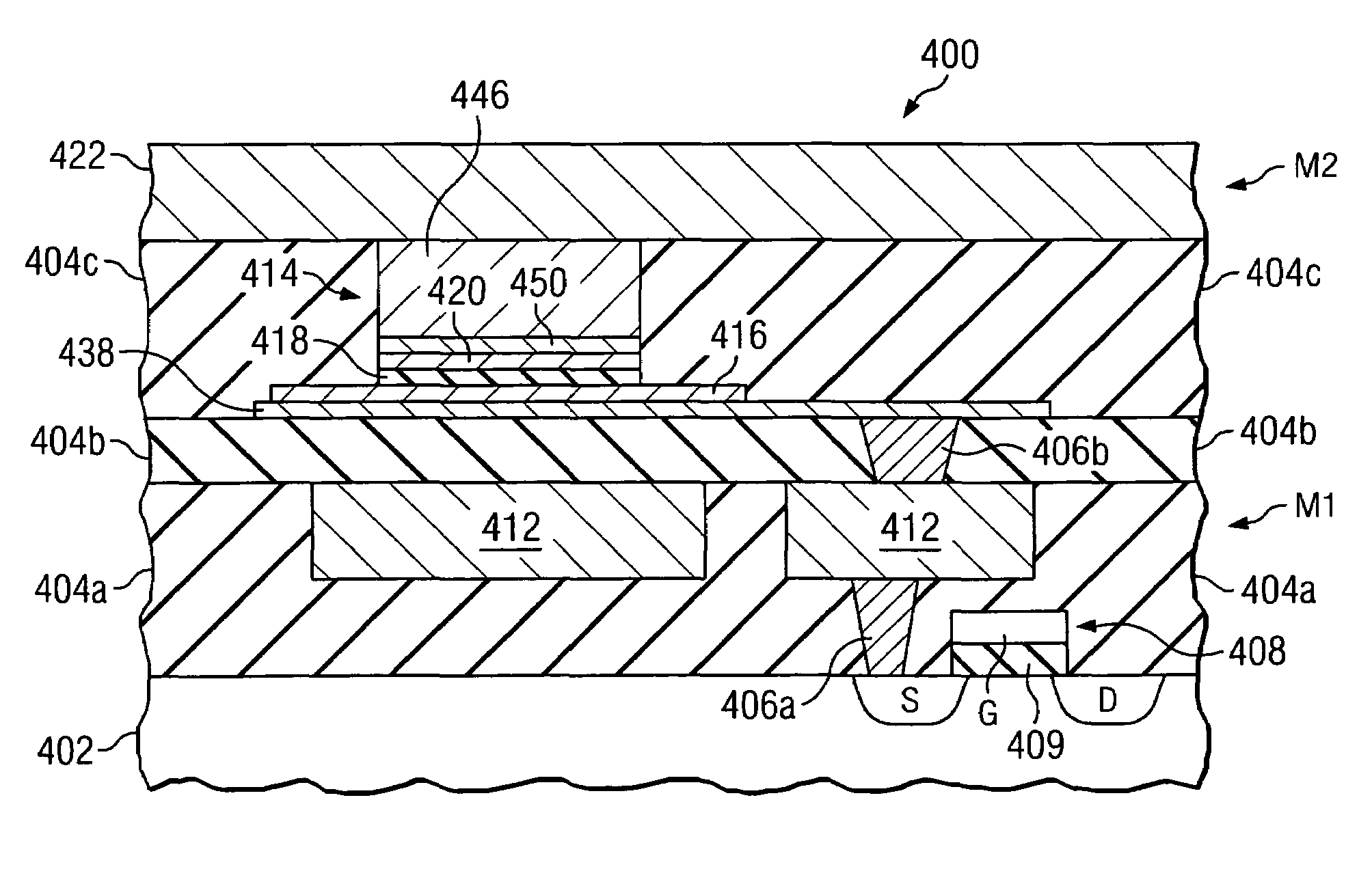
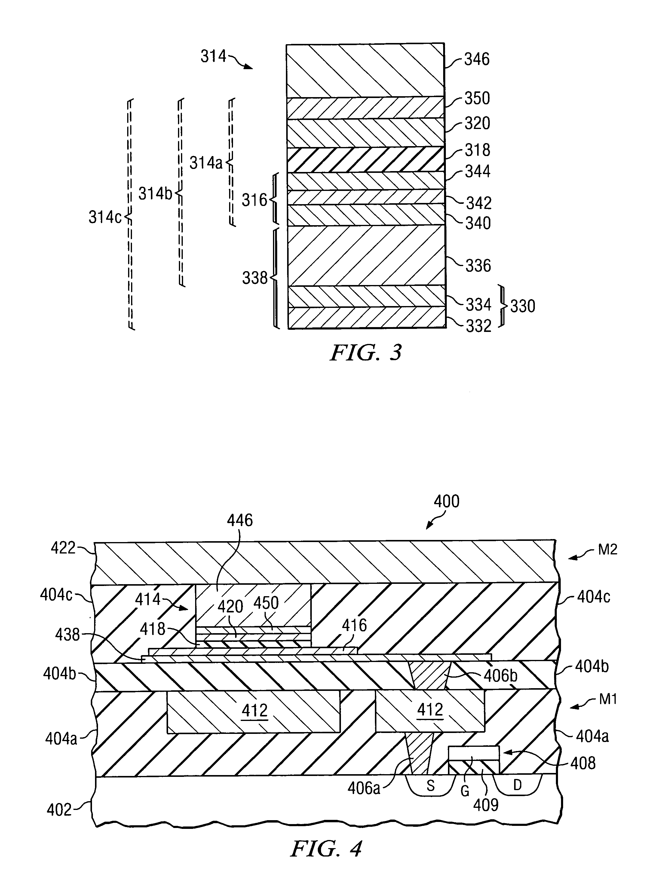
[0022]The present invention will be described with respect to preferred embodiments in a specific context, namely a magnetic stack implemented in an MRAM array. Embodiments of the present invention may also be applied, however, to other resistive memory device applications, magnetic memory cell designs, and magnetic semiconductor device applications, as examples. The present invention is particularly beneficial when implemented in the manufacture of FET and crosspoint MRAM arrays, as examples.

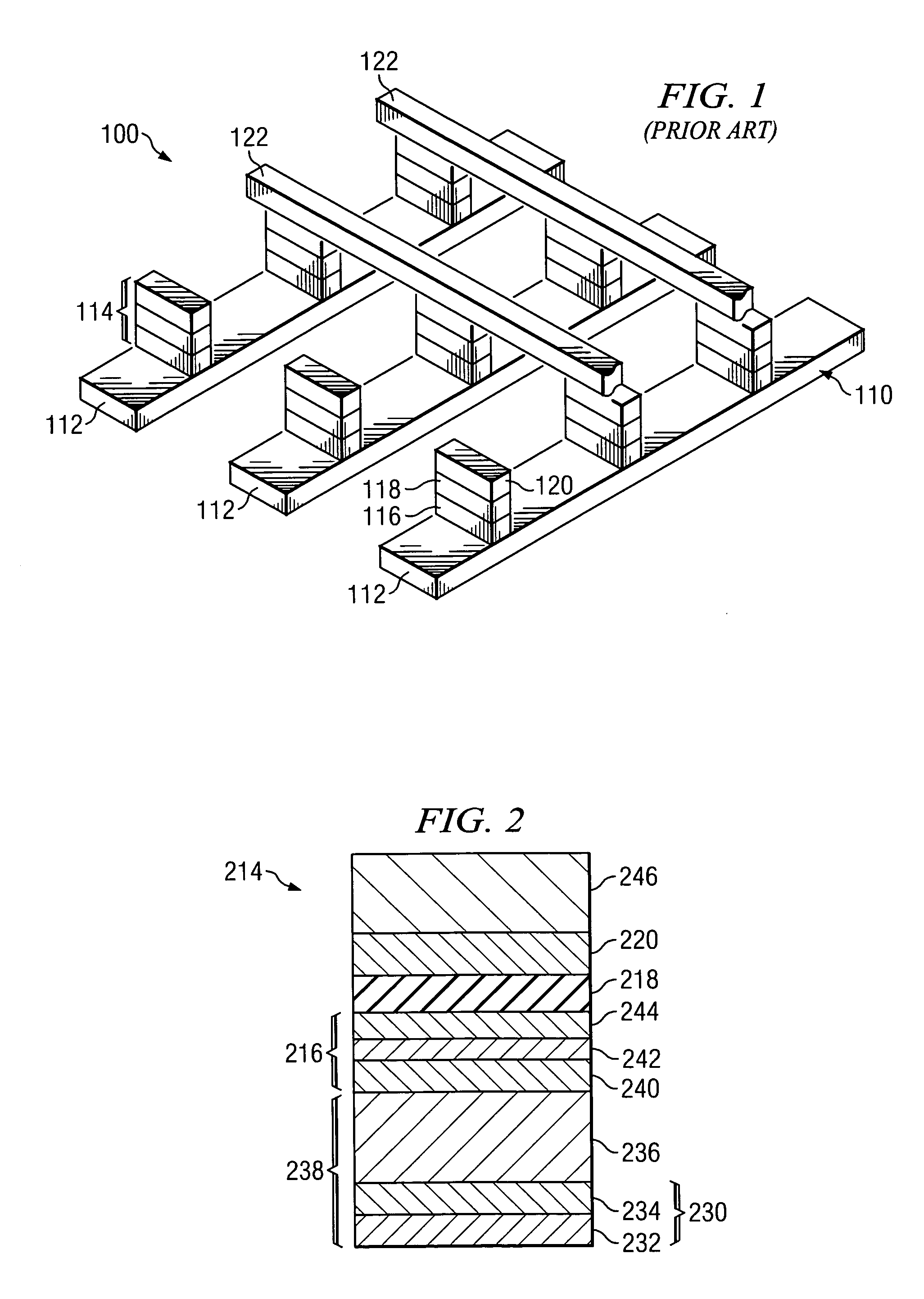
[0023]A prior art MRAM design structure will be described, followed by a discussion ...


PUM


Abstract

A method of forming a magnetic stack and a structure for a magnetic stack of a resistive memory device. A crystallization inhibiting layer is formed over the free layer of a magnetic stack, improving thermal stability. The crystallization inhibiting layer comprises an amorphous material having a higher crystallization temperature than the crystallization temperature of the free layer material. The crystallization inhibiting layer inhibits the crystallization of the underlying free layer, providing improved thermal stability for the resistive memory device.

Description

TECHNICAL FIELD[0001]The present invention relates generally to the fabrication of semiconductor devices, and more particularly to the fabrication of magnetic memory devices.BACKGROUND[0002]Semiconductors are used in integrated circuits for electronic applications, including radios, televisions, cell phones, and personal computing devices, as examples. One type of semiconductor device is a semiconductor storage device, such as a dynamic random access memory (DRAM) and flash memory, which use a charge to store information.[0003]A recent development in semiconductor memory devices involves spin electronics, which combines semiconductor technology and magnetics. The spin of electrons, rather than the charge, is used to indicate the presence of binary states “1” and “0.” One such spin electronic device is a magnetic random access memory (MRAM) device which includes conductive lines (wordlines and bitlines) positioned in a different direction, e.g., perpendicular to one another in differ...

Claims


Application Information

Patent Timeline
Patent Type & Authority Patents(United States)
IPC IPC(8): H01L21/00H01L21/8246H01L27/22H01L43/12
CPCB82Y10/00H01L27/228H01L43/12H10B61/22H10N50/01
Inventor RABERG, WOLFGANG
Owner POLARIS INNOVATIONS
Why Eureka
Try Eureka