SAR with partial capacitor sampling to reduce parasitic capacitance

a partial capacitor and parasitic capacitance technology, applied in the field of data converters, can solve the problems of noise introduction by the voltage source driving the common mode node or reference node for each input, the capacitor array weight is increased, and the noise introduction by the voltage source is cancelled, so as to achieve the effect of reducing parasitic capacitan

Inactive Publication Date: 2005-12-20
SILICON LAB INC
View PDF20 Cites 21 Cited by
  • Summary
  • Abstract
  • Description
  • Claims
  • Application Information

AI Technical Summary

Benefits of technology

[0007]The present invention described and claimed herein, in one aspect thereof, comprises an analog-to-digital convertor with reduced parasitic capacitance on the input during a sampling operation. A charge-redistribution, binary-weighted switched-capacitor array is included having a plurality of array capacitors that each have a commonly connected plate interfaced to a first common node and a switched plate, the switched plate operable to be switched between first and second reference voltages during a redistribution phase and select ones of the capacitors additionally operable to be switched to the input during a sampling phase. Each of the array capacitors has a parasitic capacitance associated therewith. A compensation capacitor having a comm

Problems solved by technology

A number of problems exist with the data conversion of an analog signal to a digital signal.
Some of these problems reside in the various offsets of the inputs to the comparators, one of which is due to the fact that the actual chip ground may be different from the input ground at the PC board on which the actual chip is disposed.
Additionally, the capacitors in the capacitor array are weighted and can have errors associated therewith.
Additionally, these capacitor arrays can also have various parasitics associated therewith that effect the operation thereof and req

Method used


Image

  • SAR with partial capacitor sampling to reduce parasitic capacitance
  • SAR with partial capacitor sampling to reduce parasitic capacitance
  • SAR with partial capacitor sampling to reduce parasitic capacitance

Examples


Embodiment Construction

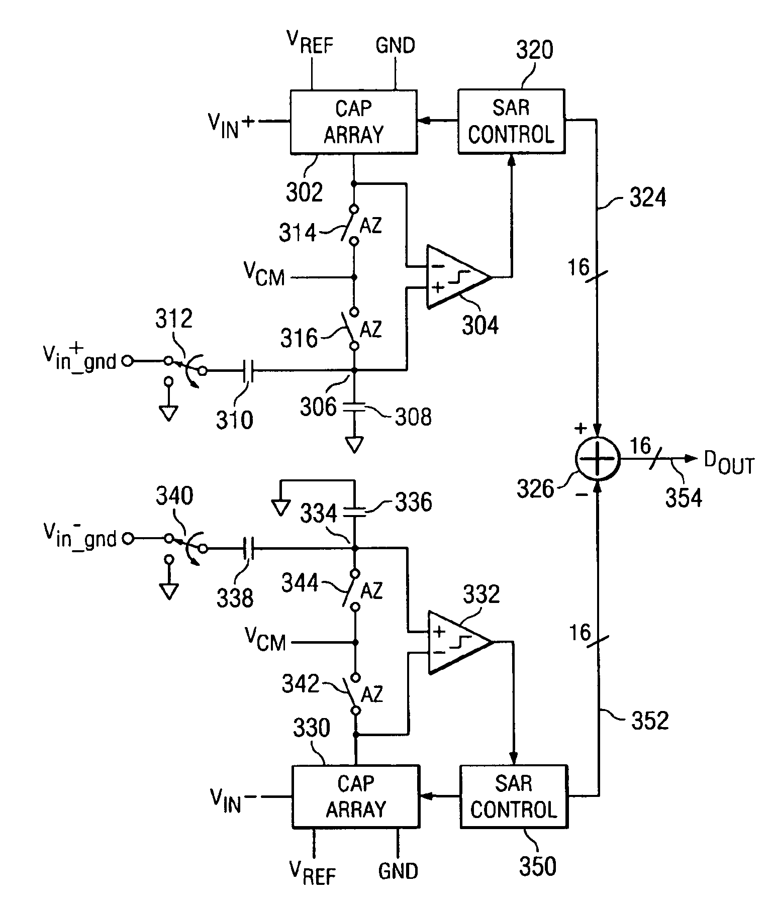
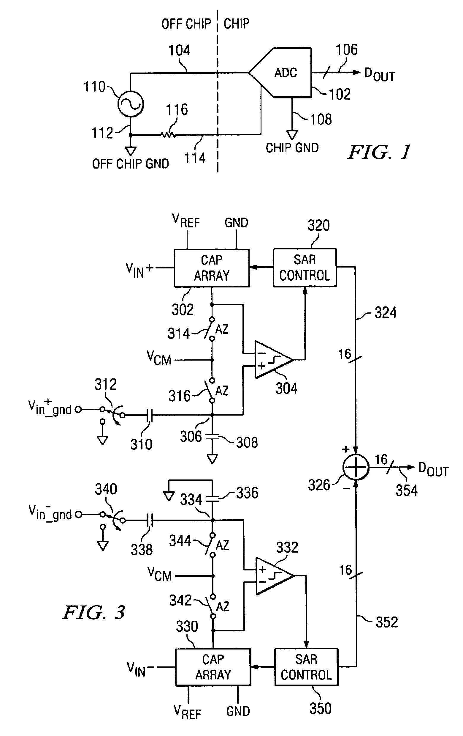
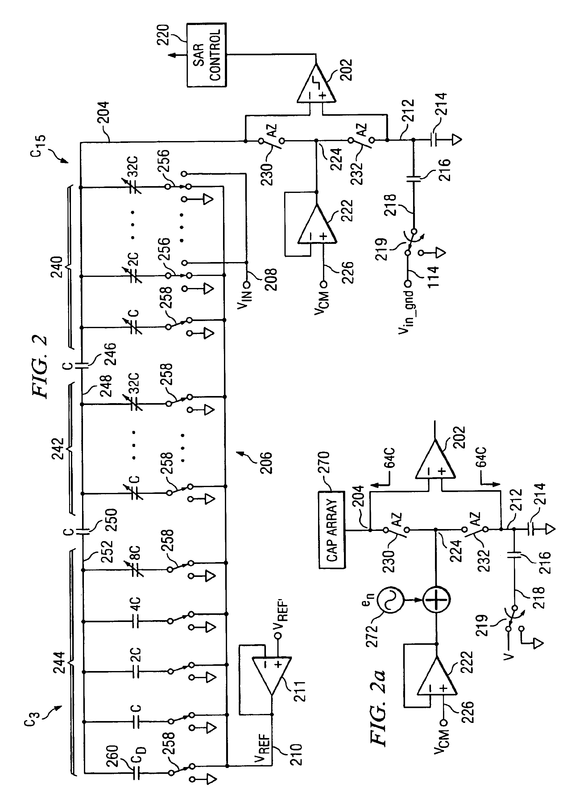
[0028]Referring now to FIG. 1, there is illustrated a diagrammatic view of an analog-to-digital convertor (ADC) 102 that is represented by a conventional ADC symbol. This ADC 102 has an analog input 104 and a digital output 106. Additionally, it is noted that ADC 102 is typically fabricated on a chip or on a PC board. Associated with the ADC 102 is a chip ground 108 that is the ground connection to the ADC 102 in proximity thereto. However, the input voltage on line 104 typically is derived from some type of external voltage source 110. Associated with that voltage source 110 is an off chip ground 112 or an off board ground. This ground is typically connected to the ADC 102 through a ground line 114, this ground line 114 having associated therewith a finite resistivity or resistance 116. As such, the voltage of the off chip ground 112 may actually be different than the chip ground 108. As will be described hereinbelow, this resistance offset in the voltage between the off chip groun...


PUM


Abstract

SAR with partial capacitor sampling to reduce parasitic capacitance. An analog-to-digital convertor is disclosed with reduced parasitic capacitance on the input during a sampling operation. A charge-redistribution, binary-weighted switched-capacitor array is included having a plurality of array capacitors that each have a commonly connected plate interfaced to a first common node and a switched plate, the switched plate operable to be switched between first and second reference voltages during a redistribution phase and select ones of the capacitors additionally operable to be switched to the input during a sampling phase. Each of the array capacitors has a parasitic capacitance associated therewith. A compensation capacitor having a common plate is connected to the first common node and a switched plate, the compensation capacitor operable to be switched to the input during the sampling phase and to the first reference voltage during the redistribution phase. The compensation capacitor has a parasitic capacitance less than the parasitic capacitance of the combination of all of the non select ones of the array capacitors. A comparator compares the voltage on the first common node to a compare reference voltage during the redistribution phase. A successive approximation controller is provided for switching the switched plate of the array capacitors between the first and second reference voltages in accordance with a successive approximation algorithm during the redistribution phase.

Description

CROSS REFERENCE TO RELATED APPLICATIONS[0001]This application is Continuation-in-Part of U.S. patent application Ser. No. 10 / 453,369, filed Jun. 3, 2003 is now a U.S. Pat. No. 6,882,298, and entitled “SAR ANALOG-TO-DIGITAL CONVERTER WITH TWO SINGLE ENDED INPUTS,” and is related to pending application entitled “NOISE CANCELLATION IN A SINGLE ENDED SAR CONVERTER,” Ser. No. 10 / 734,854; and pending application entitled “SAR DATA CONVERTER WITH UNEQUAL CLOCK PULSES FOR MSBS TO ALLOW FOR SETTLING,” Ser. No. 10 / 734,890; and pending application entitled “HIGH SPEED COMPARATOR WITH BLOCKING SWITCHES FOR SAR CONVERTER,” Ser. No. 10 / 785,164; and pending application entitled “COMMON CENTROID LAYOUT FOR PARALLEL RESISTORS IN AN AMPLIFIER WITH MATCHED AC PERFORMANCE,” Ser. No. 10 / 735,387; and pending application entitled entitled “OPEN LOOP COMMON MODE DRIVER FOR SWITCHED CAPACITOR INPUT TO SAR,” Ser. No. 10 / 734,854, all pending applications filed Dec. 12, 2003.TECHNICAL FIELD OF THE INVENTION[00...

Claims


Application Information

Patent Timeline
IPC IPC(8): G06F13/28H01C10/16H03M1/06H03M1/10H03M1/12H03M1/34H03M1/38H03M1/46H03M1/66H03M1/78
CPCH03M1/1057H03M1/468
Inventor LEUNG, KA Y.SWANSON, ERIC
Owner SILICON LAB INC
Why Eureka
Try Eureka