Solid-state imaging device

Inactive Publication Date: 2005-12-20
HAMAMATSU PHOTONICS KK
View PDF15 Cites 35 Cited by
  • Summary
  • Abstract
  • Description
  • Claims
  • Application Information

AI Technical Summary

Benefits of technology

[0012]The integrated signal outputted from the variable capacity integrator circuit is inputted to the comparator, which compares the value of the integrated signal with a reference value in terms of magnitude, whereby a comparison result signal as a result of the comparison is outputted from the comparator. The comparison result signal is inputted to the capacity control section, which controls the capacity value of the variable capacity part according to the comparison result signal. Namely, a feedback loop constituted by the variable capacity integrator circuit, comparator, and capacity control section repeatedly sets the capacity value of the variable capacity part and compares the value of integrated signal and the reference value in terms of magnitude until the capacity control section determines that the value of integrated signal and the reference value coincide with each other at a predetermined resol

Problems solved by technology

The conventional example mentioned above, however, is problematic in that the S/N ratio upon amplification is not favorable, since it does not carry out signal processing for eliminating the noise occurring upon conversion in which current signals are integrated by the integrator circui

Method used


Image

  • Solid-state imaging device
  • Solid-state imaging device
  • Solid-state imaging device

Examples


first embodiment

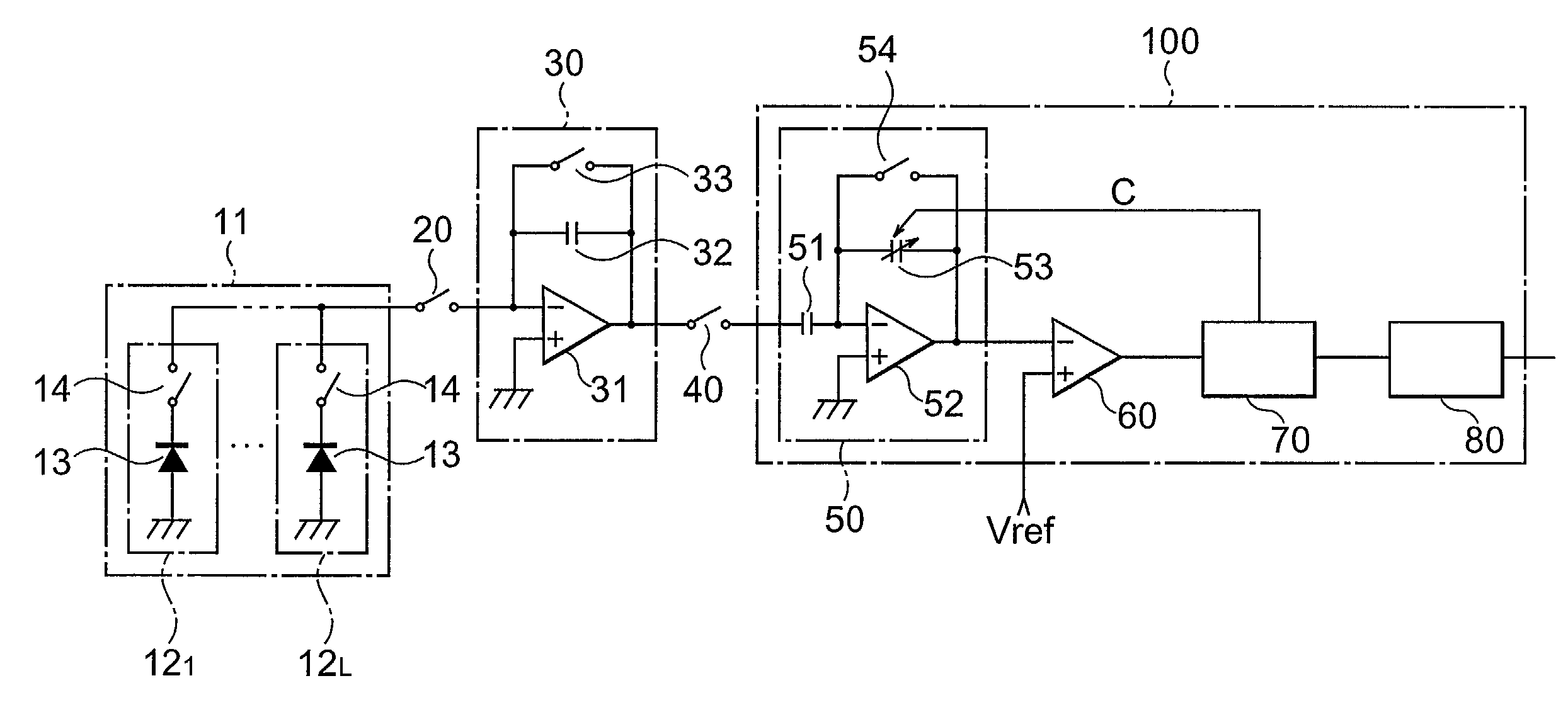
[0022](First Embodiment)

[0023]To begin with, a first embodiment of the solid-state imaging device in accordance with the present invention will be explained. FIG. 1 is a schematic circuit diagram of the solid-state imaging device in accordance with the first embodiment. This drawing shows the configuration of an individual column of a two-dimensionally arranged photodetector array or the configuration of a one-dimensionally arranged photodetector array. In the following, the configuration of an individual column of a two-dimensionally arranged photodetector array will be explained, and the individual column of the photodetector array will be referred to as a vertical photodetective section 11.

[0024]In the vertical photodetective section 11, photodetectors 12i (i=1 to L) are arranged. Each of the photodetectors 12i (i=1 to L) comprises a photoelectric conversion device 13 and a switch 14. Each of the respective photoelectric conversion devices 13 of the photodetectors 12i (i=1 to L) ...

second embodiment

[0058](Second Embodiment)

[0059]A second embodiment of the solid-state imaging device in accordance with the present invention will now be explained. FIG. 5 is a schematic block diagram of the solid-state imaging device in accordance with the second embodiment. The solid-state imaging device in accordance with this embodiment comprises a photodetective unit 10 in which vertical photodetective sections 11j (j=1 to 16) are arranged, switches 20j (j=1 to 16), integrator circuits 30j (j=1 to 16), switches 40j (j=1 to 16), shift register sections 91 to 94, and signal processing units 100j (j=1 to 4). Though the numbers of the vertical photodetective sections 11, switches 20, integrator circuits 30, and switches 40 are 16 each here, they may be provided by a greater number.

[0060]In the photodetective unit 10, photodetectors 12 are arranged two-dimensionally. Namely, in the photodetective unit 10, the photodetectors 12 are arranged in a first direction so as to form a vertical photodetectiv...

third embodiment

[0068](Third Embodiment)

[0069]A third embodiment of the solid-state imaging device in accordance with the present invention will now be explained. FIG. 6 is a schematic block diagram of the solid-state imaging device in accordance with the third embodiment. The solid-state imaging device in accordance with this embodiment comprises a photodetective unit 10 in which vertical photodetective sections 11j (j=1 to 16) are arranged, switches 20j (j=1 to 16), integrator circuits 30j (j=1 to 4), switches 40j (j=1 to 16), shift register sections 91 to 94, and signal processing units 100j (j=1 to 4). Though the numbers of the vertical photodetective sections 11, switches 20, and switches 40 are 16 each, whereas the number of integrator circuits 30 is 4 here, they may be provided by greater numbers.

[0070]In the photodetective unit 10, photodetectors 12 are arranged two-dimensionally. Namely, in the photodetective unit 10, the photodetectors 12 are arranged in a first direction so as to form a ...


PUM


Abstract

A current signal corresponding to the amount of incident light detected by a photoelectric conversion device 13 is inputted to and integrated by an integrator circuit 30, whereby a voltage signal is outputted from the integrator circuit 30. When a switch 40 is closed, the voltage signal outputted from the integrator circuit 30 is inputted to a capacitor 51 of a variable capacity integrator circuit 50, a change of the voltage signal is inputted to an amplifier 52, and an electric charge corresponding to the change of voltage signal and the capacity value of a variable capacity part 53 flows into the variable capacity part 53. The capacity value of the variable capacity part 53 is controlled by a comparator 60 and a capacity control section 70 such that the value of integrated signal outputted from the variable capacity integrator circuit 50 coincide with a reference value. The capacity control section 70 outputs a first digital signal corresponding to the capacity value of the variable capacity part 53. As a consequence, a solid-state imaging device which is excellent in S/N ratio, yields no offset errors even when its amplifier have offset fluctuations, and has a small circuit scale is obtained.

Description

RELATED APPLICATION[0001]This is a continuation-in-part application of application Ser. No. PCT / JP99 / 03675 filed on Jul. 7, 1999, now pending.BACKGROUND OF THE INVENTION[0002]1. Field of the Invention[0003]The present invention relates to a MOS type solid-state imaging device which can pickup two-dimensional light images.[0004]2. Related Background Art[0005]In the mainstream of solid-state imaging devices used in various fields such as home video are those of a charge-coupled device (CCD) type having a high sensitivity and excellent characteristics such as low noise. In special fields, however, MOS type solid-state imaging devices excellent in their efficiency of transferring electric charges generated upon incident light have been in use.[0006]Among the MOS type solid-state imaging devices, those capable of picking up two-dimensional light images have conventionally employed a system in which a number of photodetectors two-dimensionally arranged on a semiconductor chip are provided...

Claims


Application Information

Patent Timeline
IPC IPC(8): H04N5/335H04N5/341H01L27/146H04N5/357H04N5/363H04N5/369H04N5/374H04N5/378
CPCH04N5/3575H04N5/3658H04N5/378H04N25/616H04N25/677H04N25/75
Inventor MIZUNO, SEIICHIROYAMAKAWA, HIROO
Owner HAMAMATSU PHOTONICS KK
Why Eureka
Try Eureka