

Nitride based semiconductor light-emitting device
a technology of semi-conductor light-emitting device and nitride, which is applied in the direction of solid-state devices, semiconductor lasers, lasers, etc., can solve the problems of insufficient clarification of the effect of indium compositional fluctuation on device performance, and it is not easy to prepare uniform ingan amorphous films in crystal growth, etc., to achieve low threshold current, low output performance, and high output performan
- Summary
- Abstract
- Description
- Claims
- Application Information
AI Technical Summary
Benefits of technology
Problems solved by technology
Method used
Image

Examples
first example
[0255]A first example according to the present invention will be described in detail with reference to the drawings. An n-GaN substrate with a low dislocation density was prepared by the above described facet-initiated epitaxial lateral over growth. The prepared substrate was made into contact with a phosphoric acid based solution to form etching-pits. The substrate was then measured in density of the etching-pits for measuring a surface dislocation density. It was confirmed that the measured surface dislocation density was 5.0×107 cm−2.
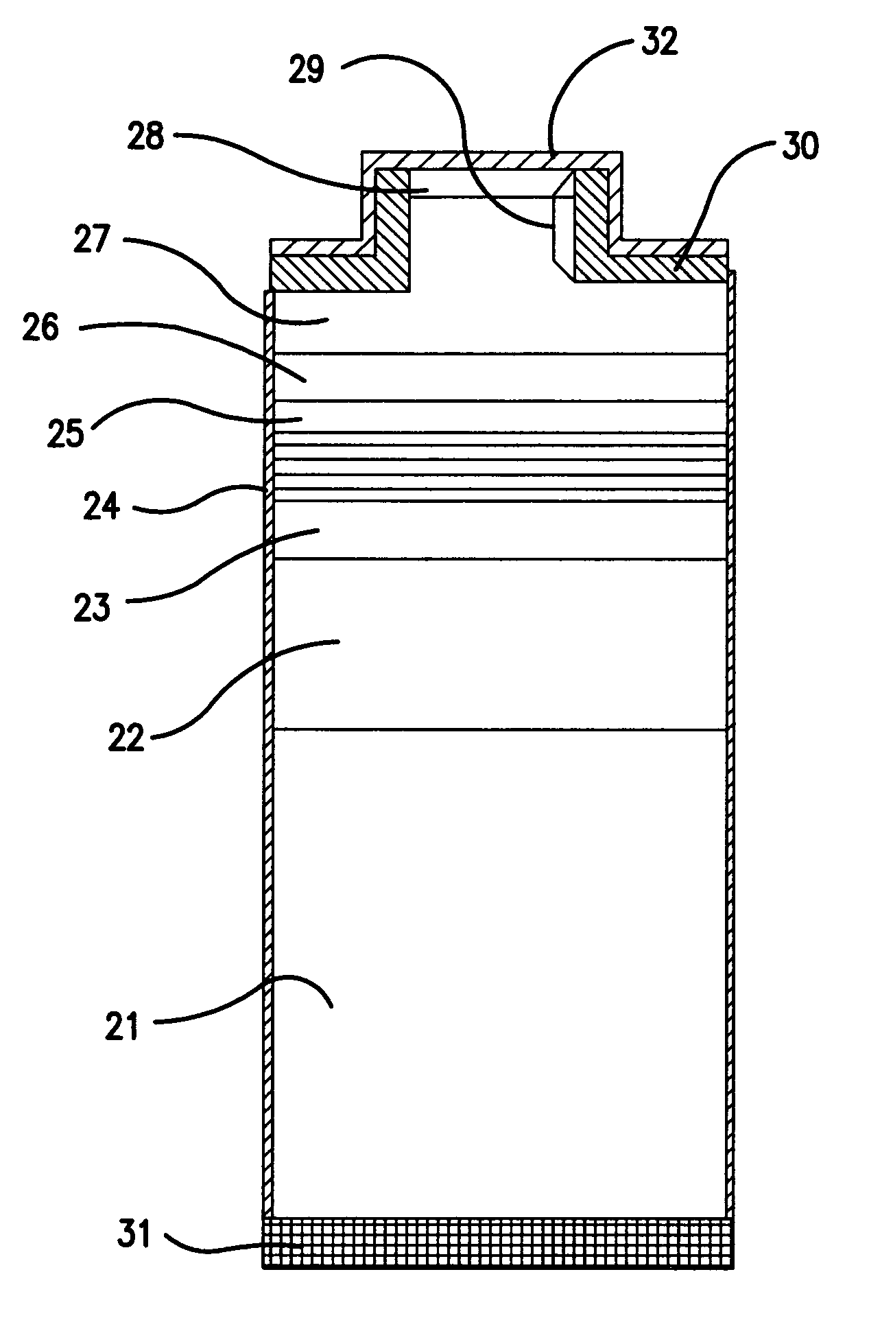
[0256]This n-GaN substrate with the low surface dislocation density was used for forming a gallium nitride based laser diode. FIG. 12A is a cross sectional elevation view illustrative of a semiconductor laser diode in a first example in accordance with the present invention. An n-type cladding layer 22 was formed on a top surface of the n-GaN substrate 21, wherein the n-type cladding layer 22 comprises an Si-doped n-type Al0.1Ga0.9N layer having a si...
second example
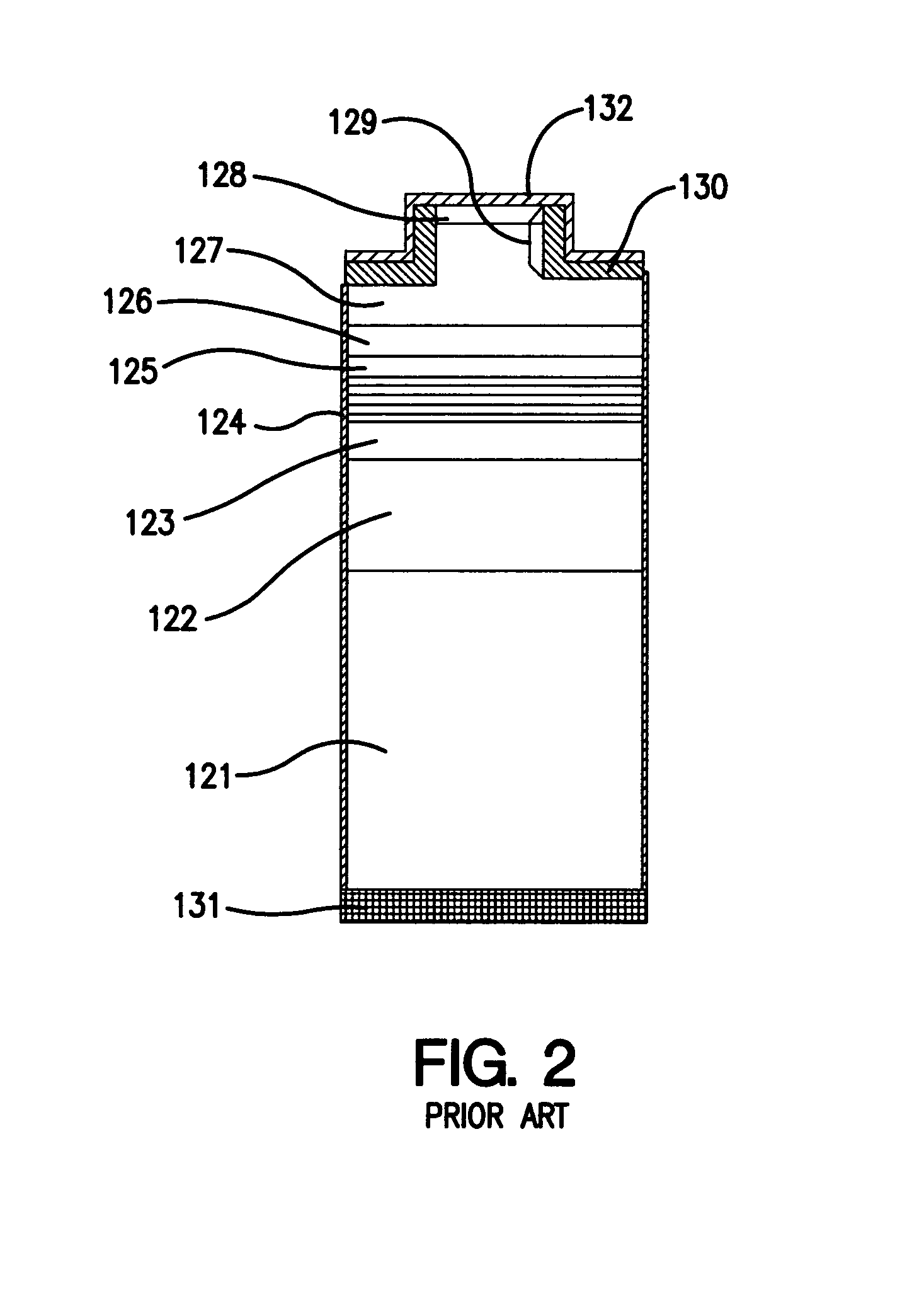
[0268]A second example according to the present invention will be described in detail with reference to the drawings. An n-GaN substrate with a low dislocation density was prepared by the above described facet-initiated epitaxial lateral over growth. The prepared substrate was made into contact with a phosphoric acid based solution to form etching-pits. The substrate was then measured in density of the etching-pits for measuring a surface dislocation density. It was confirmed that the measured surface dislocation density was 5.0×107 cm−2. The laser device of this second example is different from the first example in the high output performance and the single quantum well active layer.
[0269]This n-GaN substrate with the low surface dislocation density was used for forming a gallium nitride based laser diode. FIG. 12B is a cross sectional elevation view illustrative of a semiconductor laser diode in a second example in accordance with the present invention. An n-type cladding layer 42...
PUM
 Abstract
Description
Claims
Application Information